Skoltech researchers and their colleagues from RAS Institute for Physics of Microstructures, Lobachevsky State University of Nizhny Novgorod, ITMO University, Lomonosov Moscow State University, and A.M. Prokhorov General Physics Institute, Russia, have found a way to increase photoluminescence in silicon, the notoriously poor emitter and absorber of photons at the heart of all modern electronics. This discovery may pave the way to photonic integrated circuits, boosting their performance.
Microcircuit manufacturers have hit a wall on the way to increasing silicon CMOS chip performance because of the heat release due to high density of elements in CMOS circuits. One potential workaround is reducing heat generation by switching from metallic connections between elements in microcircuits to optical ones. Unlike electrons in conductors, photons can travel giant distances in waveguides with minimal heat losses.
“The transition to CMOS-compatible photonic integrated circuits will also make it possible to significantly increase the information transfer rate within a chip and between individual chips in modern computers, making them faster. Unfortunately, silicon itself weakly interacts with light: it is a poor emitter and a poor absorber of photons. Therefore, taming silicon to interact with light effectively is an essential task,” says Sergey Dyakov, senior researcher at Skoltech and the first author of the paper.
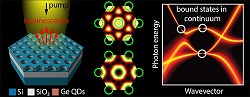
Dyakov and his colleagues have managed to enhance silicon-based photoluminescence using germanium quantum dots and a specially designed photonic crystal. They used a resonator based on bound states in the continuum, an idea borrowed from quantum mechanics. These resonators create effective confinement of light inside them since the symmetry of the electromagnetic field inside the resonator does not correspond to the symmetry of the electromagnetic waves of the surrounding space.
They also chose germanium nano-islands as a source of luminescence, which can be embedded into the desired place on a silicon chip. “The use of bound states in the continuum increased luminescence intensity by more than a hundred times,” Dyakov says, noting that it can lead us to CMOS-compatible photonic integrated circuits.
The paper, Photonic Bound States in the Continuum in Si Structures with the Self-Assembled Ge Nanoislands, was published in the journal Laser and Photonics Reviews.
Image – Silicon photonic crystal layer (left), its eigenmodes (center), and its emission spectrum (right). Courtesy of Sergey Dyakov, Sergey Tikhodeev, Nikolay Gippius.
For more information:
The Skolkovo Institute of Science and Technology
https://www.skoltech.ru/en