According to new findings by researchers at Carnegie Mellon University, Pittsburgh, a 70-year-old model used to predict the microstructure of materials doesn’t work for today’s materials. A microscopy technique developed by Carnegie Mellon and Argonne National Laboratory yields evidence that contradicts the conventional model and points the way toward the use of new types of characterizations to predict properties—and therefore the safety and long-term durability—of new materials.
Professors Gregory Rohrer and Robert Suter of Carnegie Mellon University’s Department of Materials Science and Engineering and Department of Physics have uncovered new information that will help materials scientists to predict how the properties of materials change in response to stressors such as elevated temperatures. Using near-field high energy diffraction microscopy (HEDM), they found that the established model for predicting a material’s microstructure and properties does not apply to polycrystalline materials and a new model is needed.
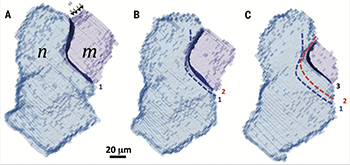
For the last 70 years, researchers have predicted materials’ behavior using a theory that says that the speed at which grain boundaries move throughout a heated material is correlated to the boundary’s shape. In an article in Science, Rohrer and Suter have shown that this theory, formulated to describe the most ideal case, does not apply to real polycrystals.
Polycrystals are more complicated than the ideal cases studied in the past. Rohrer explained, “If one considers a single grain boundary in a crystal, it can move without interruption, like a car driving down an empty roadway. In polycrystals each grain boundary is connected to, on average, ten others, so it’s like that car hit traffic—it can’t move so freely anymore. Therefore, this model no longer holds.” On top of that, Rohrer and Suter found that often polycrystal grain boundaries weren’t even moving in the direction that the model would have predicted.
HEDM, a technique that was pioneered by Suter and colleagues using the Argonne National Laboratory’s Advanced Photon Source (APS), was key to these discoveries. HEDM and its associated techniques allow researchers to non-destructively image thousands of crystals and measure their orientations within opaque metals and ceramics. The technique requires high energy x-rays available only at one of a few synchrotron sources around the world.
The development of HEDM began around 20 years ago and continues to this day. Suter’s group worked with scientists at APS to develop procedures for the synchronized collection of thousands of images of x-ray diffraction patterns from a material sample as it undergoes precision rotation in an intense incident beam. High performance computer codes developed by Suter’s research group convert the sets of images into three dimensional maps of the crystalline grains that make up the material microstructure.
While the current analysis is based on a single material, nickel, x-ray diffraction microscopy is being used on many materials and Rohrer and Suter believe that many of those materials will demonstrate similar behavior to that seen in nickel. Similar applications to other material processing conditions also are being studied.
This research was funded by the National Science Foundation’s Designing Materials to Revolutionize and Engineer the Future program (DRMEF). ASM Fellow, Elizabeth Holm, Carnegie Mellon University, Department of Materials Science and Engineering, is among additional researchers to be involved in the next steps of research studying how and why polycrystals behave this way in different materials.
Image – The dark blue shading represents a boundary separating two grains; as the boundary moves some elements that belong to grain m become part of grain n. Courtesy of College of Engineering, Carnegie Mellon University.
************
For more information: