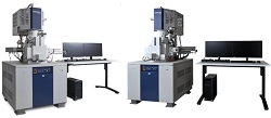
Hitachi High-Tech Corp. (“Hitachi High-Tech”), Tokyo, launched two cutting-edge field-emission scanning electron microscope models (FE-SEM), the SU8600 and SU8700 that feature new detectors, capabilities, advanced automation, and more. This class of instrumentation is used to observe, measure, define, and analyze microstructures across a wide range of fields including semiconductors, life sciences and materials development.
To be effective in such fields today, data-driven research and development requiring the acquisition of large data sets is necessary. Therefore, this product line has been designed to support the rapid acquisition of large, high-quality data sets and reduce the effort required by operators through the utilization of next-generation automation.
With today’s ever expanding application fields, the need to acquire large amounts of data in a short amount of time with minimal input has become crucial. To address this, Hitachi has re-envisioned and transformed the implementation of automated functions as well as the design of hardware components in order to support the acquisition of superb data in vast quantities with the utmost efficiency.
The SU8600 utilizes an ultra-stable cold-field emission source to enable exceptional low-energy imaging for fine structural analysis as well as high-resolution observation of beam sensitive materials like polymers. Conversely, the SU8700 employs a Schottky field-emission source to better address analytical requirements requiring high probe currents such as electron backscatter diffraction analysis on ceramics or metals.
Traditionally, FE-SEM operators have been required to change and adjust observation conditions on case-by-case basis according to the object or analytical goal. The amount of time it takes to make these adjustments depends on the operator’s proficiency and can lead to variations in data quality as well as throughput. Both the SU8600 and SU8700 now integrate functionality to automate many of these adjustment processes, creating simple, stable, high-throughput and repeatable operation.
As the capability of equipment increases, so does volume of data required. Manually collecting these substantial amounts of data can translate to more work for operators. To address this, the SU8600 and SU8700 can be equipped with an optional “EM Flow Creator” feature, which enables automatic data acquisition according to user-specific conditions and steps. This allows large-scale data sets to be acquired easily, efficiently, and automatically.
A multitude of signals can be obtained from almost any SEM, however, this product line permits the display as well as capture of up to six detector signals simultaneously, allowing operators to collect more information in less time.
Field of view (FOV) is important for maximizing data acquisition and resolution; therefore, the maximum number of pixels has been expanded to 40,960 × 30,720 pixels, an optional feature, which is 64 times that of existing models. This feature enables detailed evaluation of numerous regions of interest and localized microstructures using just a single image.
New optional detectors have been developed for the SU8600 to enhance the observation of topographical and cathode luminescence information. Also, the response speed of the new backscattered electron detector has been improved to increase throughput.
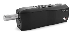
Also, the SU8700 specimen chamber is structured in such a way that it allows for energy-dispersive X-ray spectroscopy analysis at a short working distance, improving the spatial resolution of the technique and making it possible to thoroughly analyze even smaller features with greater comprehension.
Image – Field Emission Scanning Electron Microscope SU8600 (Left), SU8700 (Right)
For more information:
Hitachi High-Tech
https://www.hitachi-hightech.com/global/