For the first time, scientists have created a fully functional memory chip only a few atoms thick and integrated it into conventional chips. This advance from at Fudan University in Shanghai could pave the way for more powerful and energy-efficient electronic devices.
Decades of innovation have shrunk the circuits on a computer chip so that, nowadays, engineers can pack billions of tiny components onto a single thumbnail-sized silicon wafer. But silicon chips are now reaching the physical limits of how small they can go while still performing reliably. The solution is two-dimensional (2D) materials, which are materials that are just a single layer of atoms thick that can be scaled down even further and have superior electronic properties.
However, the problem with 2D materials like graphene up until now has been that only simple chips could be constructed with them, and it wasn’t easy to connect them to traditional processors. Now, in research published in the journal Nature, Fudan University’s Chunsen Liu and his colleagues have overcome these hurdles. They successfully combined atomically thin 2D memory cells directly onto a conventional silicon chip, creating the world’s first two-dimensional silicon-based hybrid architecture chip.
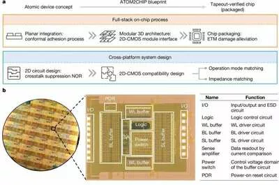
So how did they do it? The scientists created a special technique, which they call ATOM2CHIP, to grow a memory material only a few atoms thick directly onto a standard silicon chip. This solved the major engineering challenge of reliably connecting a super-thin 2D layer and communicating with the thicker silicon circuits underneath. They also developed a type of packaging to protect fragile 2D materials from stress, heat and static electricity.
To prove the chip worked, the team ran full-chip tests, clocking it running at five megahertz (MHz). They also used a test platform known as checkerboard programming to confirm every part of the memory system worked reliably.
What the researchers created wasn’t a lab prototype but a functional chip that could work in the real world. It uses very little power, is faster than older silicon memory and handles complex operations that modern systems and devices require. “These system-level results represent an important milestone in extending the superiority of 2D electronics to real-world applications,” wrote the researchers in their paper.
The work could usher in a generation of ultra-fast memory for smaller, faster and more reliable chips. That could lead to breakthroughs in advanced AI computing and fundamentally change how computers store and process information.
Image – A full-featured 2D flash memory chip enabled by ATOM2CHIP technology. Courtesy of: Nature (2025).
For more information
Fudan University
https://www.fudan.edu.cn/en/