
Toyota and Lexus have launched one of the year’s biggest recalls, affecting over a million vehicles from 2023–2026 due to a parking assist camera issue.
Continue reading

Toyota and Lexus have launched one of the year’s biggest recalls, affecting over a million vehicles from 2023–2026 due to a parking assist camera issue.
Continue reading
For the first time, scientists have created a fully functional memory chip only a few atoms thick and integrated it into conventional chips, an advance from Fudan University in China that could pave the way for more powerful and energy-efficient electronic devices.
Continue reading
Chinese researchers at Hefei University of Technology have created a paper-thin LED that gives off a warm, sun-like glow and could light up the next generation of phone and computer screens and other light sources.
Continue reading
A sharp uptick in reported counterfeit and nonconforming electronic components in 2024 has underscored a widening threat to component authenticity, according to the latest ERAI Annual Report.
Continue reading
Researchers at the Massachusetts Institute of Technology have developed a technique to create a multilayered chip with alternating layers of high-quality semiconducting material grown directly on top of one another.
Continue reading
Federal agencies would be prohibited from using certain products if they were purchased from an entity other than the original manufacturer or an authorized reseller under a new bipartisan Senate bill.
Continue reading
ElevATE Semiconductor, San Diego, Calif., and GlobalFoundries (GF) announced a manufacturing partnership for high-voltage chips produced at GF’s facility in Essex Junction, Vermont.
Continue reading
Samsung Electronics, South Korea, a world leader in advanced memory technology, developed the industry’s first LPDDR5X DRAM supporting the industry’s highest performance of up to 10.7 gigabits-per-second.
Continue reading
ZEISS, Germany, is entering into a cooperation with BORG Automotive, one of Europe’s leading independent remanufacturers of automotive parts.
Continue reading
Materials Analysis Technology Inc., Taiwan, is setting up new laboratories in Kumamoto, Japan, and the US state of Arizona to support its “big clients,” and is eyeing more locations in the future amid the changing IC supply chain landscape.
Continue reading
Samsung Electronics Co., South Korea, the world’s largest memory chipmaker, plans to unveil an advanced three-dimensional chip packaging technology to compete with foundry leader Taiwan Semiconductor Manufacturing Company.
Continue reading
Researchers from Tohoku University, Japan, used sputtering to fabricate large-area 2D vdW tetra-chalcogenides and identified an exceptionally promising material ー niobium telluride ーthat exhibits an ultra-low melting point, opening up new possibilities for developing high-performance phase change memories.
Continue reading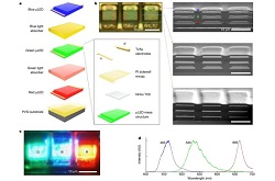 MIT engineers, Boston, Mass., have developed a new way to make sharper, defect-free displays, stacking the diodes to create vertical, multicolored pixels. Each stacked pixel can generate the full commercial range of colors and measures about 4 microns wide. The microscopic pixels, or micro-LEDs, can be packed to a density of 5,000 pixels per inch.
Over the years, the size of individual pixels has shrunk, enabling many more of them to be packed into devices to produce sharper, higher-resolution digital displays. But LEDs are reaching a limit to how small they can be while also performing effectively, especially noticeable in close-range displays such as augmented and virtual reality devices, where limited pixel density results in a “screen door effect” such that users perceive stripes in the space between pixels.
“This is the smallest micro-LED pixel, and the highest pixel density reported in the journals,” says Jeehwan Kim, associate professor of mechanical engineering at MIT. “We show that vertical pixellation is the way to go for higher-resolution displays in a smaller footprint.”
For next-generation displays, researchers are exploring inorganic micro-LEDs—diodes that are one-hundredth the size of conventional LEDs and are made from inorganic, single-crystalline semiconducting materials. Micro-LEDs could perform better, require less energy, and last longer than OLEDs.
Typical micro-LED fabrication using pick-and-place has required extreme accuracy, as microscopic pixels of red, green, and blue need to first be grown separately on wafers then precisely placed on a plate, in exact alignment with each other in order to properly reflect and produce various colors and shades. Achieving such microscopic precision is a difficult task, and entire devices need to be scrapped if pixels are found to be out of place.
The new MIT technique using vertical arrangement is an entirely different potentially less wasteful way to fabricate micro-LEDs.
The research group previously developed a method to grow and peel away perfect, two-dimensional, single-crystalline material from wafers of silicon and other surfaces—an approach they call 2D material-based layer transfer, or 2DLT.
In the current study, this approach was used to grow ultrathin membranes of red, green, and blue LEDs. They then peeled the entire LED membranes away from their base wafers, and stacked them together to make a layer cake of red, green, and blue membranes. They could then carve the cake into patterns of tiny, vertical pixels, each as small as 4 microns wide.
“In conventional displays, each R, G, and B pixel is arranged laterally, which limits how small you can create each pixel,” Shin says. “Because we are stacking all three pixels vertically, in theory we could reduce the pixel area by a third.”
The team has shown that it can grow, peel, and stack ultrathin LEDs. As a demonstration, the team fabricated a vertical LED pixel, and showed that by altering the voltage applied to each of the pixel’s red, green, and blue membranes, they could produce various colors in a single pixel.
“If you have a higher current to red, and weaker to blue, the pixel would appear pink, and so on,” Shin says. “We’re able to create all the mixed colors, and our display can cover close to the commercial color space that’s available.”
The team plans to improve the operation of the vertical pixels. So far, they have shown they can stimulate an individual structure to produce the full spectrum of colors. They will work toward making an array of many vertical micro-LED pixels.
“You need a system to control 25 million LEDs separately,” Shin says. “Here, we’ve only partially demonstrated that. The active matrix operation is something we’ll need to further develop.”
Results are published in the journal Nature.
Image – Vertically stacked, full-color µLEDs enabled by 2DLT. Courtesy of: Nature (2023).
For more information:
Massachusetts Institute of Technology
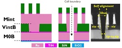 Imec, Belgium, a world-leading research and innovation hub in nanoelectronics and digital technologies, presents a semi-damascene integration approach for implementing the vertical-horizontal-vertical (VHV) scaling booster – intended to enable 4-track (4T) standard cells. The semi-damascene process enables cell boundary scaling down to 8nm tip-to-tip (T2T) in the middle-of-line (MOL) layers, providing self-aligned edges.
This provides a booster that designers can use for packing standard cells tighter, representing a 21 percent area gain over 5T designs. The novel routing scheme, along with the semi-damascene integration approach, will be critical to gradually push the logic scaling roadmap well into the Å era.
For a long time, the MOL, which provides the connection between the front-end-of-line (FEOL) and back-end-of-line (BEOL), has been organized as a single-layer contact. But currently, it is expanding into several layers, including, for example, the Mint and Vint layers. These MOL layers carry the electrical signals from the transistor’s source, drain, and gate to the local interconnects and vice versa.
Imec recently introduced a novel standard cell routing architecture called VHV, which involves the introduction of an extra MOL layer (M0B) as a scaling booster to enable 4T standard cell designs. With this booster, the first three routing layers in the standard cell follow a VHV routing style instead of the traditional HVH routing style in 5T standard cells. However, the novel two-level MOL VHV scaling booster is challenging from a process integration point of view, mainly arising from the tight boundary between neighboring 4T standard cells. The cell boundary requires a tight T2T between adjacent MOL M0B lines and two vias (VintB) facing each other with well-defined via edges – all at a minimum distance of one critical dimension (CD) of the top Mint layer. This means that the T2T and VintB via distance will need to be gradually reduced from ~24nm to ~8nm for upcoming technology nodes. This can no longer be achieved using a direct lithographic print but requires a self-aligned patterning strategy instead.
Researchers defined the tight boundary between adjacent standard cells using a two-level semi-damascene approach involving a direct metal etch. Zsolt Tőkei, program director of nano-interconnects and fellow at imec said, “Roughly speaking, we start from conventionally defined continuous lines and wider vias and, once two metal layers are finished, we split them into two, using the top 16-18nm pitch Mint layer as a hard mask for the final patterning step. This results in 3 edges (of Mint, VintB, and M0B) that are simultaneously self-aligned. With our Ru-based two-level test vehicle, we obtained an average via CD of 10.5nm and M0B T2T as tight as 8.9nm – a key achievement.” Imec researchers complemented structural validation with an initial electrical characterization of line resistance and isolation properties.
“The VHV routing scheme is a critical scaling booster to enable cell boundaries at the A10, A7, A5, A3 technology nodes,” adds Tőkei. “It also applies to future device architectures such as nanosheet, forksheet, and CFET. By extending semi-damascene from the BEOL towards the MOL, we have now also found a way to integrate this promising booster. More detailed investigations will, however, be needed, and for that purpose, imec is taping out a new dedicated mask.”
Image – (Left/middle) Schematic representation of the semi-damascene process flow used to test the key features of VHV. (Right) TEM image of the test vehicle after the final Ru etch: T2T M0B and VintB via are self-aligned to the 18mn pitch Mint layer.
For more information:
Imec
 Applied Materials, Inc., Santa Clara, Calif., announced “Singapore 2030” – a multi-faceted plan to expand its operations in Singapore over the next eight years. The plan is targeted at strengthening the company’s global manufacturing and R&D capabilities, broadening technology ecosystem partnerships in Singapore and promoting local workforce development.
“For the past 30 years, Singapore has been a strategic hub for Applied Materials, and we are excited to build on our success with new investments that will strengthen our ability to support the semiconductor industry on its path to becoming a US$1 trillion market by the end of the decade,” said Gary Dickerson, president and CEO of Applied Materials. “We look forward to working with the Government of Singapore and the vibrant technology ecosystem to create opportunities for mutual growth that will benefit the global semiconductor industry.”
With the semiconductor industry entering a new wave of growth fueled by digital transformation of the economy, Applied has announced its intention to make multi-billion-dollar investments in its innovation infrastructure in the United States and to expand its global manufacturing capacity. As part of Singapore 2030, Applied Materials held a groundbreaking ceremony for an expansion of its regional hub in Singapore, which is home to Applied’s largest factory outside of the United States. This investment of hundreds of millions of U.S. dollars will strengthen the company’s ability to meet growing customer demand in the years ahead.
In addition, the company will invest to bolster its R&D capabilities in Singapore with a focus on accelerating commercialization of new technologies and services that improve chip power, performance, area, cost and time-to-market (PPACt). One example is the research collaboration between Applied and the Institute of Microelectronics (IME), a research institute of Singapore’s Agency for Science, Technology and Research (A*STAR), focused on hybrid bonding and other emerging, 3D chip integration technologies.
As a top employer, Applied will help enable a future-ready workforce for Singapore’s semiconductor equipment industry through enhanced training and advanced education programs. This includes an initiative with the Singapore Institute of Technology where Applied employees gain access to tailored learning modules in areas including AI and machine learning, smart manufacturing, robotics and automation, data science, and more.
Applied Materials established its presence in Singapore in 1991 with a small sales and service site that has grown to become a major manufacturing and regional operations hub with a workforce of more than 2,500. In 2019, Applied received the Distinguished Partner in Progress Award from the Government of Singapore in recognition of the company’s outstanding contributions and commitment to the country.
For more information:
Applied Materials, Inc.
 Researchers in Drexel University’s College of Engineering have developed a thin film device fabricated by spray coating that can block electromagnetic radiation with the flip of a switch. The breakthrough, enabled by versatile two-dimensional materials called MXenes, could adjust the performance of electronic devices, strengthen wireless connections, and secure mobile communications against intrusion.
The team previously demonstrated that two-dimensional layered MXene materials – discovered just over a decade ago – when combined with an electrolyte solution, can be turned into a potent active shield against electromagnetic waves. This latest MXene discovery, reported in Nature Nanotechnology, shows how this shielding can be tuned when a small voltage – less than that produced by an alkaline battery – is applied.
MXene is a unique material in that it is highly conductive making it perfectly suited for reflecting microwave radiation that could cause static, feedback, or diminish the performance of communications devices. But its internal chemical structure can also be temporarily altered to allow these electromagnetic waves to pass through.
This means that a thin coating on a device or electrical components prevents them from both emitting electromagnetic waves, as well as being penetrated by those emitted by other electronics. Eliminating the possibility of interference from both internal and external sources can ensure the performance of the device, but some waves must be allowed to exit and enter when it is being used for communication.
The key to eliciting bidirectional tunability of MXene’s shielding property is using the flow and expulsion of ions to alternately expand and compress the space between material’s layers, like an accordion, as well as to change the surface chemistry of MXenes.
With a small voltage applied to the film, ions enter – or intercalate – between the MXene layers altering the charge of their surface and inducing electrostatic attraction, which serves to change the layer spacing, the conductivity and shielding efficiency of the material. When the ions are deintercalated as the current is switched off, the MXene layers return to their original state.
The team tested 10 different MXene-electrolyte combinations, applying each via paint sprayer in a layer about 30 to 100 times thinner than a human hair. The materials consistently demonstrated the dynamic tunability of shielding efficiency in blocking microwave radiation, which is impossible for traditional metals like copper and steel. And the device sustained the performance through more than 500 charge-discharge cycles.
These results indicate that the MXene films can convert from electromagnetic interference shielding to quasi-electromagnetic wave transmission by electrochemical oxidation of MXenes. The MXene film can potentially serve as a dynamic EMI shielding switch.
For security applications, the team suggests that the MXene shielding could hide devices from detection by radar or other tracing systems. The team also tested the potential of a one-way shielding switch. This would allow a device to remain undetectable and protected from unauthorized access until it is deployed for use.
The next step for the team is to explore additional MXene-electrolyte combinations and mechanisms to fine-tune the shielding to achieve a stronger modulation of electromagnetic wave transmission and dynamic adjustment to block radiation at a variety of bandwidths.
For more information:
Drexel University