Researchers from the Fermi National Accelerator Laboratory-led Superconducting Quantum Materials and Systems Center, or SQMS, in Batavia, Illinois, have completed one of the most comprehensive studies ever conducted, linking materials and their structures — including surfaces, interfaces and geometries — to variations in quantum device performance. This research provides new insights that directly connect to device fabrication, an important step on the path toward building practical and reliable quantum computers.
In a large-scale study involving Fermilab, Northwestern University, Rigetti Computing, Ames National Laboratory, National Institute of Standards and Technology, and National Physical Laboratory, SQMS researchers examined 22 superconducting transmon qubits fabricated by Fermilab, Rigetti and NIST.
Using seven different materials-characterization techniques, the teams documented the material properties of quantum devices exhibiting varying levels of quantum-state coherence and investigated correlations with device-performance data.
The study was designed to remove bias from the process, and researchers who characterized the devices did not know how the qubits had performed. Instead, each team examined the devices, documented the features they observed and quantified those features as thoroughly as possible. Only after the data was collected did researchers look for correlations between materials defects and variations in qubit performance.
The analysis pointed to three features that stood out in relation to variations in device performance: the depth of the trenches around device structures, the angle of the etched sidewalls and the thickness of the oxide layer on the surface.
- Surface oxide-layer thickness reflects the chemistry of the superconducting surface. Prior SQMS work showed this layer, though only a few nanometers thick, dominates losses in niobium qubits. This study adds that even single nanometer variations in oxide thickness from device-to-device can meaningfully shift performance.
- Sidewall angles are tied to how device structures are patterned and etched during fabrication. Electromagnetic simulations indicate that a sharp angle of approximately 10-15 degrees reduces the electric field stored in lossy oxides and predicts improvement in performance by 20 to 30% compared to a broader, more tapered angle of around 30 degrees.
- Trench depth was also found to significantly contribute to variations in qubit performance. This represents the vertical distance of the recesses etched into the underlying substrate — the foundation of the qubit — immediately adjacent to the edges of the superconducting metal electrodes. At trench depths below approximately 20 nanometers, small variations have a more dramatic effect on device performance. At a larger trench depth, this effect saturates and other factors play a more prominent role. Like sidewall angles, trench depths are also tied to fabrication.
Across the devices studied, differences in these three features accounted for as much as a twofold variation in performance among qubits fabricated from identical materials. This evidence therefore points to tighter control over trench depth, sidewall angle and oxide thickness as a way to narrow that spread.
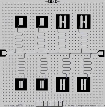
Image – This superconducting transmon chip measures 7.5 millimeters by 7.5 millimeters and contains eight qubits. SQMS researchers fabricate these chips at the Pritzker Nanofabrication Facility at the University of Chicago. Courtesy of: SQMS Center, Fermilab.
For more information:
Fermi National Accelerator Laboratory
www.fnal.gov