A research team at Penn State has uncovered a potential method for precisely manipulating a material’s properties by altering its atomic arrangement. Their discovery suggests that “atomic spray painting” of potassium niobate, a material commonly used in advanced electronics, can finely tune the resulting thin films. This technique, detailed in Advanced Materials, could lead to environmentally friendly innovations in consumer electronics, medical devices, and quantum computing.
The technique, known as strain tuning, alters a material’s characteristics by compressing or stretching its atomic unit cell—the repeating pattern of atoms that defines its crystal structure.
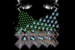
The scientists used Molecular Beam Epitaxy (MBE), a process that forms a thin film by depositing individual atomic layers onto a substrate. In this case, they created a strain-tuned thin layer of potassium niobate.
“This was the first time potassium niobate has been grown using MBE. The technique is like spray-painting atoms onto a surface,” says Venkatraman Gopalan, study Corresponding author, Pennsylvania State University.
The researchers state that the novel MBE technique, combined with a crystal acting as a substrate template, generates the strain required to tune the material.
This method allows the atoms in the thin films to adjust to the underlying substrate’s atomic structure, causing strain. Even a tiny stretch of about 1 % can create pressure that would be impossible to achieve by simply pulling or pressing on such a brittle material from the outside.
This pressure can significantly improve how the material works from a ferroelectric perspective.
Potassium niobate is a ferroelectric material. It has a natural electric polarization that can be reversed by applying an external electric field, similar to how a magnet’s polarization can be flipped with an external magnetic field.
Strain engineering involves layering two materials with slightly different atomic sizes. When atoms are deposited onto a surface composed of atoms with a slightly different spacing, the new layer will compress or stretch to align with the surface beneath it, provided the layer is thin enough.
This strain, similar to the way a rubber band stretches when pulled, alters the material’s properties. It can raise temperature limits or enhance ferroelectric performance, depending on the size and spacing of the atoms in the underlying surface.
“The superior strength of coupling between strain and polarization in potassium niobate compared to other ferroelectrics allows for a unique opportunity where relatively small amounts of strain can result in colossal tuning of both the ferroelectric structure and its polarization,” says Sankalpa Hazra, doctoral candidate and study co-author, Pennsylvania State University.
Hazra continued, “A primary consequence of this superior strain sensitivity is that the ferroelectric performance of potassium niobate can be remarkably enhanced, even surpassing those of lead titanate or lead zirconate titanate, which are considered to be industrial standard levels of ferroelectricity for device applications.”
While potassium niobate is lead-free, it is particularly significant for demonstrating strain tuning. Many of the most effective ferroelectric materials, such as lead titanate and lead zirconate titanate, contain lead, despite its known environmental and health risks.
The study suggests that potassium niobate could be a safe, environmentally friendly alternative with strong ferroelectric properties. However, without strain tuning, its ferroelectric performance is typically weaker than its lead-based counterparts.
The research also revealed that strain-tuned potassium niobate maintained its ferroelectric performance even at high temperatures. This is noteworthy, as heat usually disrupts ferroelectric materials, causing them to lose polarization and preventing them from switching electrical charge.
“In our work, we have shown that applying strain can increase the temperature at which the material loses its ferroelectric properties. What is even more impressive is that with just a 1% strain, we can push that temperature to over 975 ºK, which is close to the point where the material starts to degrade,” Gopalan said.
According to the researchers, the next “serious hurdle” for practical applications is growing these thin films on silicon, which is widely used in the electronics industry. By optimizing the film growth process, Gopalan’s team is also attempting to enhance the material’s electrical characteristics.
This could allow strain-tuned potassium niobate to be utilized in practical applications, including high-temperature memory storage for space exploration, quantum computing, and more sustainable high-tech devices.
“With further development, this novel version of the material could become a key player in the next generation of green, high-performance technologies that impact everything from our devices to space exploration,” Gopalan said.
**************************************************************
Image – “Atomic spray painting” of potassium niobate, a material commonly used in advanced electronics onto a substrate, could enable the tuning of properties of the resulting thin film, according to a new study. Courtesy of: Jennifer M. McCann.
For more information:
The Pennsylvania State University