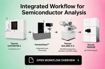
Tescan, Czech Republic, unifies non-destructive Micro-CT, ultrafast laser processing, and high-precision FIB-SEM into a single, integrated workflow to accelerate root-cause determination in advanced semiconductor packaging while minimizing preparation-induced artifacts.
In advanced semiconductor packaging, the primary challenge is often not defect detection itself but efficiently reaching buried regions of interest without introducing preparation-induced artifacts. As packages become increasingly heterogeneous and vertically integrated, failure analysis workflows must balance localization accuracy, preparation speed, and preservation of device integrity across multiple analytical instruments.
That is where the combination of Micro-CT, ultrafast laser processing, and Focused Ion Beam – Scanning Electron Microscopy (FIB-SEM) becomes especially valuable.
- Micro-CT provides non-destructive insight into buried structures, and its 3D data can serve as a navigational map for identifying the region of interest (ROI).
- Laser processing enables fast targeted access to such ROIs, but should do so without inducing damage.
- FIB-SEM delivers the final precision milling, imaging, and analytical investigation needed for detailed investigation.
When integrated into a coordinated workflow, these technologies reduce rework, shorten time-to-data, and improve the repeatability and reliability of advanced failure analysis.
Micro-CT enables non-destructive volumetric inspection prior to destructive preparation, helping teams identify buried structures such as solder voids, TSV defects, delamination regions, and interconnect failures. Although spatial resolution and material contrast can vary depending on package composition and size, 3D CT data provide valuable navigation context that reduces destructive trial-and-error during downstream preparation.
FemtoChisel is designed for this step. It operates in the non-thermal ablation regime and is built to reach deeply buried regions of interest without microcracks, melt zones, or redeposition, while delivering reproducible, analysis-ready results across advanced semiconductor devices.
FemtoChisel’s correlative machine vision and in-process depth monitoring further strengthen this step. FemtoChisel can use CT, SEM, or optical data for navigation and targeting, while its integrated nanometer-resolution confocal height sensor supports endpoint precision during processing.
Tescan FIB-SEM systems combine high-resolution SEM imaging with precise ion beam milling to support both structural characterization and advanced analytical workflows. Depending on the application, users may select Ga FIB for high-precision nanoscale work or Xe plasma FIB for faster large-volume material removal, allowing the workflow to be optimized for either ultimate precision, throughput, or a balance of both.
In advanced packaging workflows, this level of precision is what transforms physical access into meaningful analytical insight. Clean cross-sections and site-specific preparation across structures such as BGAs, TSVs, MEMS, and OLED devices enable more accurate root-cause analysis while minimizing preparation-induced artifacts. By incorporating FemtoChisel upstream for rapid bulk access, the FIB-SEM can focus less on large-volume material removal and recovery steps, and more on the high-resolution imaging, precision polishing, and analytical characterization needed to fully understand the failure mechanism.
The strength of this workflow is not just that each tool performs well on its own. It is that each tool handles the part of the job it is best suited for. Micro-CT localizes the problem non-destructively. FemtoChisel opens access quickly and cleanly. FIB-SEM completes the final preparation and analysis with nanometer-scale control. Together, they reduce the friction between steps and make the overall process more efficient and more reliable.
For more information:
Tescan
https://tescan.com