Intel Corp., Santa Clara, Calif., devised a process to manufacture, test, and demonstrate positive performance results with its new backside power solution called PowerVia, enabling chipmaking to go two-sided for the first time.
This new approach to delivering power required a radical rethink to both how chips are made and how they are tested. Typically microchips are built from the bottom up, in layers, including wires among the top layers that bring in the power that makes the chip go. When the chip is done, they are flipped over and are enclosed in packaging that provides connections to the outer world.
Unfortunately, this approach is running into problems. As they get smaller and denser, the layers that share interconnects and power connections have become an increasingly chaotic web that hinders the overall performance of each chip. Power and signals fade, requiring workarounds or simply dumping more power in.
Research and development on the backside power solution that Intel and leading-edge chipmakers are all working toward dates back a decade. This approach moves the power wires below the transistor to the back side of the chip leaving the front side cleanly focused only on interconnection.
Ben Sell, vice president of technology development at Intel and part of the team that brought PowerVia to fruition, explains how it works. Transistors are built first, as before, with the interconnect layers added next. Now the fun part: flip over the wafer and “polish everything off,” Sell notes, to expose the bottom layer to which the metal layers for power will be connected. “We call it silicon technology,” he adds, “but the amount of silicon that’s left on these wafers is really tiny.”
After the polish, “now you only have very few metal layers and they’re all very thick,” Sell explains — remember he lives in the land of nanometers, so “thick” means mere micrometers. That leaves “a very direct path for the power delivery to your transistor.”
The benefits of this approach are manifold, Sell confirms, surpassing the added complexity of the new process.
The wires for power, for example, can take up to 20% of that front-side real estate, so with them gone, the interconnect layers can be “relaxed.” “That more than offsets the cost of this whole big process,” Sell notes, simplifying what had been the most tortuous portion of the manufacturing flow. The net effect is that the two-part flip-it-over process is actually cheaper than the old way.
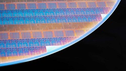
The benefits aren’t limited to manufacturing. The test chip the Intel team used to prove out the approach — called Blue Sky Creek and based on the Efficient-core (E-core) coming in Intel’s forthcoming Meteor Lake processor for PCs — demonstrated that PowerVia solved both problems caused by the old method. With separated and fatter wires for power and interconnection, “you get better power delivery and you get better signal wiring,” says Sell.
For your average computer user, this means more efficient speed. Get work done faster and with less power, the promise of Moore’s Law delivered again. The Intel E-core designed with PowerVia demonstrates >5% frequency improvement and >90% cell density with acceptable debug times as Intel 4. Sell confirms this is a “substantial” frequency boost for just moving wires around.
Today, chip-testing techniques are based on the accessibility of the transistors in that first and lowest layer. With the transistors now sandwiched in the middle of the chip, “a lot of those techniques had to be redeveloped,” says Sell.
“Acceptable debug times” — is a critical achievement alongside the product improvements. “We have made tremendous progress over the last couple of years in developing those debug capabilities and proving them on Blue Sky Creek,” Sell asserts.
Intel doesn’t usually make test chips as functional and complete as Blue Sky Creek. In this case, the teams needed to verify not only that they could build and test a chip this way, but also that the new configuration wouldn’t bring new issues into the final product.
For instance, heat. “Normally you use the silicon side also for heat dissipation,” Sell explains. “So now you have sandwiched your transistors and the question is, ‘Do we have a thermal problem? Do we get a lot of local heating?’” At this point you can probably guess the answer: no.
“What was most amazing,” Sell recalls, “was despite these radical changes” — sandwiching transistors in the middle of the chip and introducing this heavy “polishing” to the process — “we could make the transistors look very, very close to what we had in Intel 4.”
The first opportunity to feel the many benefits of PowerVia will come in 2024 in the form of Arrow Lake, a next-generation Intel processor for PCs built using the Intel 20A process. Its billions of transistors will be inverted, working more efficiently than ever.
******************************************************************************************
Image – Wafer holds Blue Sky Creek test chips. The production test helps Intel refine Intel’s PowerVia backside power technology. Expected as part of the Intel 20A manufacturing node in 2024, PowerVia will be the industry’s first implementation of backside power in silicon, solving decades of interconnect bottlenecks. Courtesy of: Intel Corporation.
For more information:
Intel Corporation