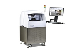
Lasertec U.S.A., San Jose, Calif., introduces the WASAVI Series BGM300. This instrument measures silicon wafer thicknesses and TSV depths prior to back grinding 3D semiconductor devices. In production, the backside of a silicon wafer needs to be properly ground to expose embedded TSVs. However, excessive grinding, may cause copper contamination. If grinding is insufficient, the subsequent etching process will become long and costly.
Furnished with the proven and reliable interferometer and new IR optics, BGM300 has overcome the challenges associated with pre-grinding TSV depth measurement. Unlike indirect measurement methods such as scatterometry, BGM300 does not require complicated calculations or previews of multiple samples against a database, and is applicable to a variety of TSV shapes and pattern layouts. It provides reliable and flexible measurement capabilities throughout development and production stages of 3D semiconductor devices.
BGM300 can also measure remaining silicon thickness (RST) over TSVs after grinding. It combines newly developed IR optics with an interferometer used on Lasertec’s MPM series, which is acclaimed as an industry standard of phase shift measurement systems among photomask manufacturers and users.
Since visible light used by most commercially available measurement systems have limited penetration depths into wafers, they are not desirable for the pre-grinding measurement. Conventional IR optics-based systems also have difficulty with TSV depth measurement due to spot size limitations.
http://www.lasertec.co.jp/en/products/semiconductor/wafer/bgm300.html