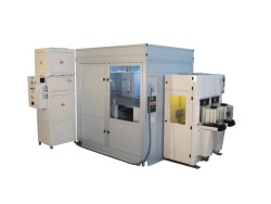
SUSS MicroTec, Germany, announces the extension of a joint development agreement with the IBM Corporation to further develop, enhance, and propel the application of excimer laser technologies in the realm of advanced semiconductor packaging, including 3D systems integration. SÜSS MicroTec Photonic Systems Inc., a subsidiary of SÜSS MicroTec, recently installed an ELP300 excimer laser stepper system at IBM.
The installation of the excimer laser system, and the JDA extension under this alliance, will serve to further develop, enhance and propel the application of Excimer laser technologies in the realm of advanced semiconductor packaging – including 3D systems integration. This joint development effort will leverage joint resources from IBM’s packaging expertise and SUSS MicroTec Photonic Systems’ 24 years of excimer laser processing and tool development to create leading-edge packaging and enable higher performance back-end-of-line materials for the semiconductor back-end.
The excimer laser process offers extended capability beyond traditional manufacturing approaches, while at the same time potentially reducing cost of ownership by extending the technology to both current and future applications.
In the program, both IBM and SUSS MicroTec will continue collaboration on the development of excimer laser processes and process systems for two distinct roles: Seed Layer Removal for UBM (under bump metallization) and micro-structuring organic dielectrics (Vias and RDL trenches) for system interconnects.
“We see high growth potential for this technology, and will continue contributing to the development of alternative processes that address manufacturing challenges and continued cost reductions.” says Frank P. Averdung, President and CEO of SUSS MicroTec. “Together with IBM, we intend to extend these capabilities to meet industry needs.”