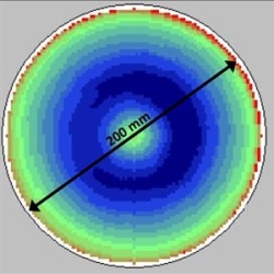
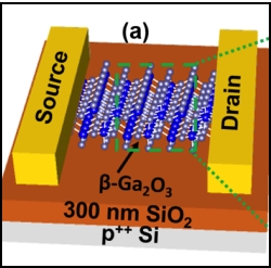
A team of researchers at the University of Illinois at Urbana-Champaign has advanced gallium nitride (GaN)-on-silicon transistor technology by optimizing the composition of the semiconductor layers that make up the device. Working with industry partners Veeco and IBM, the team created the high electron mobility transistor (HEMT) structure on a 200-mm silicon substrate with a process that will scale to larger industry-standard wafer sizes.
Can Bayram, an assistant professor of electrical and computer engineering (ECE), and his team have created the GaN HEMT structure on a silicon platform because it is compatible with existing CMOS manufacturing processes and is less expensive than other substrate options such as sapphire and silicon carbide.
However, silicon does have its challenges. Namely, the lattice constant, or space between silicon atoms, does not match up with the atomic structure of the GaN grown on top of it.
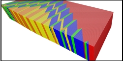
“When you grow the GaN on top, there’s a lot of strain between the layers, so we grew buffer layers [between the silicon and GaN] to help change the lattice constant into the proper size,” explained ECE undergraduate researcher Josh Perozek. Mr. Perozek is lead author of the group’s paper, “Investigation of structural, optical, and electrical characteristics of an AlGaN/GaN high electron mobility transistor structure across a 200mm Si(1 1 1) substrate,” in the Journal of Physics D: Applied Physics.
Without these buffer layers, cracks or other defects will form in the GaN material, which would prevent the transistor from operating properly. Specifically, these defects — threading dislocations or holes where atoms should be – ruin the properties of the two-dimensional electron gas channel in the device. This channel is critical to the HEMTs ability to conduct current and function at high frequencies.
http://engineering.illinois.edu/news/article/21035