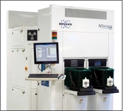
Bruker Semiconductor Division, Billerica, Mass., announces that leading multiple semiconductor manufacturers have ordered JVSensus-600E X-ray diffraction imaging systems for in-line wafer monitoring of crystalline defects. The JVSensus-600E tool is equipped with both high speed and high resolution X-ray diffraction imaging (XRDI) measurement capabilities. This enables detecting and classifying a wide range of crystalline defects induced by high-stress processes such as fast annealing and CMP, or by poor wafer handling.
Applications include monitoring edge damage to prevent costly wafer breakage during ultra fast anneal. It can qualify and monitor process tools at any technology node, which reduces cycle times and facilitates fab expansion. The JVSensus system allows defects to be identified prior to annealing, which is often the critical step that leads to wafer breakage and severe yield loss. By detecting defects early in the process, semiconductor manufacturers can quickly identify the root cause of processes causing wafer breakage, thus reducing yield loss.