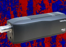
Zeiss, Germany, announces a new suite of high-resolution 3D x-ray imaging solutions for failure analysis of advanced semiconductor packages, including 2.5/3D and fan-out wafer-level packages. The new systems include the Xradia 600-series Versa and Xradia 800 Ultra x-ray microscopes (XRM) for submicron and nanoscale package FA, respectively, as well as the new Xradia Context microCT. With the addition of these new systems to its existing family of products, Zeiss says that it now provides the broadest portfolio of 3D x-ray imaging technologies serving the semiconductor industry.
The new suite of 3D x-ray imaging solutions provides submicron and nanoscale 3D images of features and defects buried within intact structures in advanced package 3D architectures. This is enabled by rotating a sample and capturing a series of 2D x-ray images from different perspectives, followed by reconstruction of 3D volumes using sophisticated mathematical models and algorithms.
An unlimited number of virtual cross-sections of the 3D volume may be viewed from any angle – providing valuable insight of failure locations prior to physical failure analysis (PFA). The combination of submicron and nanoscale XRM solutions provides a unique FA workflow that can significantly enhance FA success rates. The new Xradia Context microCT offers high contrast and resolution in a large field of view, using projection-based geometric magnification, and is fully upgradable to Xradia Versa.