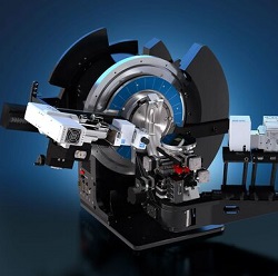
MTi Instruments, Albany, N.Y., has developed the Proforma 300i SA, a benchtop/desktop, semi-automated wafer measurement system for semi-conducting and semi-insulating materials.
Based on MTII’s exclusive Push-Pull capacitance technology, the Proforma 300i SA delivers full wafer surface scanning for thickness, thickness variation, bow, warp, and global flatness. User-defined and ASTM/SEMI compliant scan patterns are used to generate full three-dimensional wafer images.
To address the needs of the semiconductor industry, MTII developed its unique “push-pull™” probe technology. In this design, each probe consists of two capacitance sensors, built into one probe body. Each sensor is driven at the same voltage; however, there is a 180-degree phase shift between signals.
This shift allows the current path to travel across the target surface rather than through the target to ground, eliminating any inaccuracies created by poorly grounded targets. Additionally, highly non-conductive targets can be measured with this technology, thus allowing capacitance sensors to be used on semi-insulating and semi-conducting targets.
Because the Proforma 300i SA is semi-automated, an operator simply loads the semiconductor wafer onto the measurement stage and then presses a button on the machine. After 30 seconds of measurement, the Proforma 300i SA stops. The measurements are displayed on an external computer that’s interfaced to the desktop metrology system. Windows-based software shows detailed information about the wafer. User-defined and ASTM/SEMI compliant scan patterns are used to generate full 3D wafer images.