Researchers at the Department of Energy’s Oak Ridge National Laboratory have developed SimuScan, an artificial intelligence framework that uses realistic synthetic data to train AI to identify nanoscale features and autonomously target the most informative regions of a sample.
Continue readingBruker invests in Photothermal AFM-IR to advance semiconductor research
Bruker Corporation, Billerica, Mass., announced accelerated development of its photothermal AFM-IR spectroscopy capabilities to address research challenges facing the semiconductor industry as device architectures continue to shrink and systems become increasingly more complex.
Continue readingThis new chip survives 1300°F (700°C) and could change AI forever
Researchers at the University of Southern California have unveiled a new memristor memory device that continues to operate at 700 degrees Celsius (~1300 degrees Fahrenheit), marking it as the most robust high-temperature memory technology ever demonstrated.
Continue readingNew editors for Metallurgical and Materials Transactions
ASM International, Materials Park, Ohio, and The Minerals, Metals & Materials Society (TMS), Warrendale, Pa., announced two new editors for the Metallurgical and Materials Transactions journals: Steven J. Zinkle, FASM, of Oak Ridge National Laboratory (ORNL) and Sridhar Seetharaman of the University of Warwick. Zinkle Named Editor for Metallurgical and Materials Transactions E Steven J.
Continue readingMusical manuscript restored with x-rays
Scientists at Stanford University, Calif., x-rayed a damaged musical score to reveal the musical notes hidden beneath a layer of black carbon. The beautifully bound 1797 Luigi Cherubini opera Médée looks like an impeccably preserved relic of opera’s golden age. However, the final pages of the aria “Du trouble affreux qui me dévore” (“The terrible disorder that consumes me”) are blackened with carbon that completely obscures the closing lines.
Continue readingStacking up: A new take on diamond electronics
Researchers at the U.S. Department of Energy’s Argonne National Laboratory have overcome a critical barrier in diamond-based electronics and microelectronics by using nanotechnology to integrate two-dimensional materials for efficient n-type doping, a breakthrough in electronic materials designed to operate in high-temperature environments and other harsh environments.
Continue readingDetecting ‘hidden defects’ that degrade semiconductor performance with 1,000X higher sensitivity
A joint research team at the Korea Advanced Institute of Science and Technology and IBM T. J. Watson Research Center, Yorktown Heights, N.Y., has developed a new analysis method that can detect “hidden defects” in semiconductors, electronic traps that interfere with electrical flow, with approximately 1,000 times higher sensitivity than existing techniques.
Continue readingHitachi High-Tech announces the SU9600: Next-generation ultrahigh-resolution SEM with high throughput
Hitachi High-Tech Corporation, Japan, has launched the Ultrahigh-Resolution Scanning Electron Microscope SU9600, which allows for highly accurate and precise observation of substances down to the sub-nano level.
Continue readingThese contacts let you see in the dark with your eyes closed
Scientists have developed innovative contact lenses that allow both humans and mice to see infrared light by converting it into visible colors—without the need for bulky equipment or batteries. These transparent lenses enable users to perceive both regular and infrared light simultaneously and can detect multiple infrared wavelengths at once. Remarkably, the lenses perform even better with eyes closed due to infrared light’s superior penetration. In tests, mice avoided infrared light, and humans could interpret flickering codes and light directions, showcasing the lenses’ potential for practical applications.
“Our research opens up the potential for non-invasive wearable devices to give people super-vision,” says senior author Tian Xue, a neuroscientist at the University of Science and Technology of China. “There are many potential applications right away for this material. For example, flickering infrared light could be used to transmit information in security, rescue, encryption or anti-counterfeiting settings.”
The lenses use specially engineered nanoparticles that absorb invisible infrared light and convert it into light our eyes can see, typically in the 400 to 700 nanometer range. More specifically, the technology targets near-infrared light, which lies just beyond human vision, in the 800 to 1600 nanometer range.
In earlier studies, the team showed these particles could give mice infrared vision when injected directly into the eye. This time, they’ve achieved similar results using a much less invasive approach—by building the particles right into soft contact lenses.
To create the contact lenses, the team combined the nanoparticles with flexible, non-toxic polymers that are used in standard soft contact lenses. After showing that the contact lenses were non-toxic, they tested their function in both humans and mice.
They found that contact lens-wearing mice displayed behaviors suggesting that they could see infrared wavelengths. For example, when the mice were given the choice of a dark box and an infrared-illuminated box, contact-wearing mice chose the dark box whereas contact-less mice showed no preference. The mice also showed physiological signals of infrared vision: the pupils of contact-wearing mice constricted in the presence of infrared light, and brain imaging revealed that infrared light caused their visual processing centers to light up.
In humans, the infrared contact lenses enabled participants to accurately detect flashing morse code-like signals and to perceive the direction of incoming infrared light. “It’s totally clear cut: without the contact lenses, the subject cannot see anything, but when they put them on, they can clearly see the flickering of the infrared light,” said Xue.
“We also found that when the subject closes their eyes, they’re even better able to receive this flickering information, because near-infrared light penetrates the eyelid more effectively than visible light, so there is less interference from visible light.”
An additional tweak to the contact lenses allows users to differentiate between different spectra of infrared light by engineering the nanoparticles to color-code different infrared wavelengths. For example, infrared wavelengths of 980 nm were converted to blue light, wavelengths of 808 nm were converted to green light, and wavelengths of 1,532 nm were converted to red light. In addition to enabling wearers to perceive more detail within the infrared spectrum, these color-coding nanoparticles could be modified to help color blind people see wavelengths that they would otherwise be unable to detect.
“By converting red visible light into something like green visible light, this technology could make the invisible visible for color blind people,” says Xue.
Because the contact lenses have limited ability to capture fine details (due to their close proximity to the retina, which causes the converted light particles to scatter), the team also developed a wearable glass system using the same nanoparticle technology, which enabled participants to perceive higher-resolution infrared information.
Currently, the contact lenses are only able to detect infrared radiation projected from an LED light source, but the researchers are working to increase the nanoparticles’ sensitivity so that they can detect lower levels of infrared light.
“In the future, by working together with materials scientists and optical experts, we hope to make a contact lens with more precise spatial resolution and higher sensitivity,” says Xue.
For more information: Cell

Two-faced solar panels can generate more power at up to 70% less cost
Researchers at the University of Surrey, England, University of Cambridge, the Chinese Academy of Sciences, Xidian University, and Zhengzhou University, China, built a new kind of two-faced (bifacial) solar panel using single-walled carbon nanotubes as both front and back electrodes that are the highest efficiency single junction solar cells to date.
Continue readingSematech and Exogenesis form alliance for accelerated neutral atom beam technology
Sematech, Albany, N.Y., and Exogenesis Corp., Billerica, Mass., have agreed to a strategic alliance to commercialize the Exogenesis Accelerated Neutral Atom Beam (ANAB) process technology and the nAccel accelerated particle beam equipment platform.
Continue readingInnovnano invests in facility for nanostructured powders
Innovnano, Lisbon, Portugal, has invested in a high-tech, brand new facility for production of its nanostructured powders, including 3 and 4 mol % yttria stabilized zirconia (YSZ). The new site is based in a dedicated technology park in Coimbra, Portugal, and has been designed to allow high capacity expansion and industrial-scale nanotechnology, enabling the production of up to 1000 metric tons per annum.
Continue readingUniversity of Albany Nano College to become a separate institution
State University of New York, Albany, N.Y., announces that the pioneering College of Nanoscale Science and Engineering will become a separate institution within the SUNY system by the 2014-15 academic year. The establishment of SUNY CNSE will further cement New York’s position as a global center for nanotechnology innovation, high tech industry and research, and unmatched educational opportunities.
Continue readingHitachi launches transmission electron microscope with improved electro-optics.
Hitachi High-Technologies Corp., Tokyo, introduces the HT7800 Series Transmission Electron Microscope, which features digital operation under normal room light conditions (like the HT7700 model) and also incorporates improved electro-optics with many new functions.
Continue readingWafer surface measurement based on capacitance technology generates 3D images
MTi Instruments, Albany, N.Y., has developed the Proforma 300i SA, a benchtop/desktop, semi-automated wafer measurement system for semi-conducting and semi-insulating materials.
Continue readingNCMS launches nanomanufacturing survey
The National Center for Manufacturing Sciences (NCMS) has partnered with the National Science Foundation under the National Nanotechnology Initiative (NNI) to launch its latest study of commercialization trends in nanotechnology and nanofabrication.
Continue readingInterplay of free electrons: Tailored electron pulses for improved electron microscopy
Researchers at the Max Planck Institute for Multidisciplinary Sciences, Germany, resolved and analyzed the mutual repulsion between individual electrons in an electron microscope for the first time, enabling the team to develop a method that could increase the performance of established electron microscopes and open up a new interface between electron microscopy and quantum technology.
Continue readingAddressing the nation’s need for strong domestic semiconductor industry and infrastructure
Last year, UC Riverside scientists and colleagues at UC Irvine received $5 million from the U.S. Department of Energy, to team up with Sandia National Laboratory in building a diverse educational pipeline in the field of microelectronics. Developing expertise and infrastructure in this field is a priority for industry and government.
Continue readingArtificial neurons based on semiconductor technology
Artificial neural networks are a key technology in the domain of AI and machine learning. Many applications need the rapid parallel processing of vast amounts of data—with correspondingly high energy demand. A new project in which physicist Dr. Andreas Tittl plays an important role, is seeking to develop an energy-saving alternative through a specially tailored combination of materials science and photonics.
Continue readingResearchers use nanoparticles to increase light frequency and resolution of imaging systems
Physicists at the Australian National University are using nanoparticles to develop new sources of light that increase the frequency of light that cameras and other technologies see by up to seven times.
Continue readingKnots smaller than human hair make materials unusually tough
In the latest advance in nano- and micro-architected materials, engineers at Caltech, Pasadena, Calif., developed a new material made from numerous interconnected microscale knots that made the material far tougher than identically structured but unknotted materials.
Continue readingCharged ions melt nano gold nuggets
In experiments conducted at TU Wien, Vienna, extremely small pieces of gold, consisting of a few thousand atoms and with a diameter in the order of ten nanometers, are bombarded with highly charged ions. This makes it possible to change the shape and size of these gold pieces in a targeted manner. The effects of the ion bombardment were then studied in an atomic force microscope with surprising results.
Continue readingGraphene grows—and we can see it
Graphene is extremely strong and good at conducting heat and electrical currents, making it an exceptionally versatile material. Yet, many properties of the material are still poorly understood – for the simple reason that the atoms they are made up of are very difficult to observe. A team of researchers from the University of Amsterdam (UvA) and New York University have now found a surprising way to solve this issue.
Continue readingResearchers identify effects of heat in materials with atomic resolution
A team of researchers at the University of California, Irvine, the Massachusetts Institute of Technology, and other institutions used cutting-edge electron microscopes and novel techniques to discover a way to map phonons—vibrations in crystal lattices—in atomic resolution, enabling deeper understanding of the way heat travels through quantum dots, engineered nanostructures in electronic components.
Continue readingSurprising speed-dependent friction with graphene
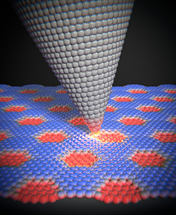
The speed at which an atomic force microscope moves across the surface of certain materials is influenced by the frictional properties of the substrate. One such example is graphene, which consists of a single layer of carbon atoms in a honeycomb arrangement. It is being examined with a view to potential use as a lubricating layer. Applications where a reduction of friction is desired include hard disks or moving components for satellites or space telescopes.
Previous studies have shown that a graphene ribbon can be moved across a gold surface with almost no friction. But if graphene is applied to a platinum surface, it has a significant impact on the measurable friction forces. Now, physicists from the University of Basel and Tel Aviv University have reported in the journal Nano Letters (“Velocity Dependence of Moiré Friction”) that, in this instance, the friction depends on the speed at which the tip of an atomic force microscope (AFM) is moved across the surface.
This finding is surprising because friction does not depend on speed according to Coulomb’s law, which applies in the macro world.
In conjunction with the platinum substrate, graphene no longer forms only the hexagonal honeycomb pattern of carbon atoms and instead forms superstructures known as Moiré superlattices. The surface is then no longer completely flat and exhibits a certain degree of roughness.
“If we move the AFM tip across this slightly corrugated surface at low speed, we measure a weak and almost constant frictional force,” explains Professor Ernst Meyer from the Swiss Nanoscience Institute and the Department of Physics at Basel University. “Above a certain threshold, however, the friction then increases with the speed of the AFM tip,” adds first author Dr. Yiming Song. “The larger the Moiré superstructure, the lower the threshold at which the friction becomes speed-dependent.”
The researchers found that there is greater resistance at the ridges of the Moiré superstructures during the movement of the tip. These ridges undergo elastic deformation due to the pushing tip before relaxing again when the pressure is sufficiently high. This effect results in greater frictional forces that increase with the speed of the tip. Simulations and an analytical model confirm the experimental findings obtained by this international team of researchers.
Image – The friction between the tip of an atomic force microscope and the Moiré superstructures depends on the speed at which the tip is moved across the surface. Courtesy of University of Basel.
************
For more information:
New imaging method makes microrobots visible in the body
Researchers at the Max Planck ETH Center for Learning Systems, Germany, have developed an imaging technique that for the first time recognizes cell-sized microrobots individually and at high resolution in a living organism.
Continue readingHow quantum light squeezes the noise out of microscopes
Lasers are often used to look at objects in microscopes. But even the best laser has “quantum noise” that makes a picture blurry and hides the details. This in turn results in measurements that are less precise than scientists need.
Continue readingU.S. DOD funds nanotechnology to protect against lasers
U.K. technology company, Advanced Material Development, has been awarded a U.S. Department of Defense (DOD) contract to develop protective films to be integrated into protective eye wear.
Continue readingUAH researchers develop new atomic layer deposition process using ultrasonics
Researchers at the University of Alabama in Huntsville invented a new way to deposit thin layers of atoms as a coating onto a substrate material at near room temperatures.
Continue readingNanomotors controlled with laser light
A team of scientists led by researchers at the Institute of Industrial Science, the University of Tokyo (UTokyo-IIS), Tokyo, Japan, designed novel linear nanomotors that can be moved in controlled directions using light.
Continue reading