Scientists at École Polytechnique Fédérale de Lausanne (EPFL) in Switzerland have made an important discovery about the structure of barium titanate, a material used in everyday objects. Their findings refute existing theories on the displacement of the material’s atoms.
Barium titanate is a ferroelectric material used in nearly all electronic devices—computers, smartphones and even electric cars. It’s used to make the sensors and capacitors they run on, for example. “A single smartphone generally has around 700 capacitors containing barium titanate, and trillions of these capacitors are made every year,” says Dragan Damjanovic, an EPFL professor and head of the Group for Ferroelectrics and Functional Oxides at EPFL’s School of Engineering. Despite barium titanate’s widespread use, however, researchers still don’t fully understand how it works. “There are of course theoretical models out there, but some of their key predictions have never been experimentally confirmed. So that’s what we set out to do,” says Damjanovic.
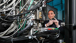
Emad Oveisi, a senior scientist at EPFL’s Interdisciplinary Center for Electron Microscopy, suggested that Damjanovic use his center’s Titan Themis—one of the world’s most powerful electron microscopes—for his research. The Titan Themis enabled the scientists to observe the atomic structures of barium titanate and barium-strontium titanate in the cubic phase. That was back in 2015, when they obtained the first images; it took another five years to analyze and verify their results. “Until now, researchers believed that the atoms move in several directions in a very short timeframe. But our experiments showed that they tend to prefer certain directions, meaning there are nanometric-sized areas where all the atoms move in the same way. That completely changes how we view these materials and their atomic structure,” says Oveisi.
Thanks to the advanced image analysis methods, the scientists were able to identify where in the material the atoms move in an orderly fashion. “When we talk about movements, we’re actually referring to displacements that take place on a picometer scale—that is, one order of magnitude smaller than the atoms themselves,” says Oveisi. Damjanovic adds: “Even though the displacements are extremely small, they have repercussions on a much larger scale. For instance, if we expose the nanometric areas we identified to a high-frequency electric field like those in smartphones, the areas heat up.” His team’s findings could therefore be extremely useful in better understanding energy loss in these kinds of materials.
“The next step will be to develop materials where the size of the displacement area is minimized in order to enhance the material’s properties,” says Damjanovic.
Image – Emad Oveisi with the Titan-Themis microscope. Courtesy of Alain Herzog/2021 EPFL.
************
For more information: