Research at Catalan Institute of Nanoscience and Nanotechnology (ICN2), Spain, and the Ecole Polytechnique Fédérale (EPFL) of Switzerland demonstrated that high-quality zinc phosphide (Zn3P2) crystals, free of interface defects, can be fabricated with a nanoscale approach. Zn3P2 nanowires were grown by selective area epitaxy (SAE), a material of interest for application in solar and photovoltaic cells. This work also used state-of-the-art microscopy techniques and 3D simulations to thoroughly investigate the formation of differently-oriented structures within the nanowires.
Zn3P2 is a semiconductor whose properties, including the abundance of its components on Earth, a direct bandgap, and a high capacity to absorb light in the visible range, make it an attractive candidate for use in solar cells as an absorber, i.e., the layer that produces free charge carriers as a result of light absorption. However, in-depth studies on it are limited because of the difficulties involved in fabricating high-quality material. In particular, crystals of Zn3P2 are produced by epitaxial growth on a substrate, but the structural characteristics of this material make it hard to grow extended bulks of it without incurring in defects, which can hamper its performance.
The study, published in Nanoscale, uses a nanostructure fabrication strategy to produce nanowires of Zn3P2 with reduced elastic strains, which results in much less defects at the interface with the substrate. Besides proving that this approach is favorable, the work also uses advanced microscopy, imaging and simulation techniques to analyze the growth process down to the atomic level and to investigate the characteristics and influence of other kind of irregularities appearing in the grown nanowires.
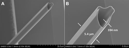
The researchers grew Zn3P2 nanowires on a substrate of indium phosphide (InP) by SAE, a technique in which a mask limits the growth to specifically designed openings and desired directions. A small contact surface between the two materials and using a mask allowed nanowires to be fabricated with no misfit dislocations at the interface, or in other words, no interface-related defects. Two nanowire crystalline orientations were grown at 45 degrees with respect to each other, and both exhibited the same high quality.
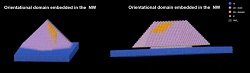
There are other defects that can show up during the fabrication process, even using this nanoscale approach, that are actually more difficult to monitor and control. In fact, the authors observed the formation of rotated domains in the grown material, meaning there are parts within the whole structure that present a different crystal orientation with respect to the rest. In order to analyze this phenomenon in detail and how it affects the quality of the Zn3P2 nanowires, the authors of this study used state-of the art techniques (atomic resolution aberration corrected high-angle annular dark-field scanning transmission electron microscopy imaging, or AC-HAADF STEM) to collect structural information about the material down to the atomic level. They also used the data collected to create reliable 3D atomic models performing HAADF-STEM image simulation, to get deeper insight into the growth process.
They observed domains rotated 120 degrees in both kinds of nanowires (at crystalline orientations of 0 and 45 degrees) whose interfaces are very sharp. No dangling bonds or mid-gap electronic states formed at the rotated interface. They explained this phenomenon as a result of the simultaneous and independent growth of crystals with different orientations in separated parts of the mask openings. As growth continues, all parts merge in a unique structure and the dominant one completely integrate the others.
This study demonstrates that the nanoscale approach based on selective area epitaxy guarantees the fabrication of higher-quality Zn3P2 crystals, i.e. growth with no defects at the interface. It also proves the capabilities of advanced microscopy, AC HAADF-STEM imaging, and 3D atomic modeling and image simulations to fully understand the defect formation and their impact on novel materials.
Image – Zn3P2 nanowires on InP at 0 and 45 degree orientation Courtesy of: Catalan Institute of Nanoscience and Nanotechnology
For more information:
Catalan Institute of Nanoscience and Nanotechnology