 ACE Solution, Taiwan, the leader and the provider in customized test solutions to meet customer needs in electrical components, devices and system manufactures, launched the TZ6000 – a nondestructive wafer quality measurement tool for the compound semiconductor industry. Incorporated with TeraPulse Lx technologies from TeraView, United Kingdom, the TZ6000 achieves nondestructive wafer quality measurements of thickness, refractive index, resistivity, dielectric constant, surface/subsurface defects at selected positions and whole wafer scanning map.
Dr. JC Chen, VP of R&D of ACE Solution, commented “The quality of the semiconductor wafer determines the maximum achievable conversion efficiency to the final device. Subsurface damages (SSD) of semiconductor wafers are easily induced during surface machining process includes rough grinding, fine grinding, and chemical mechanical polishing. Current wafer inspection systems which rely on VIS/IR/UV optical inspection can analysis the surface properties of the wafer but not the SSD, due to their low penetration depth. Terahertz (THz) wave has higher penetration depth in semiconductor wafers as silicon, silicon carbide and gallium nitride. We developed the THz-based TZ6000 to meet the market need of nondestructive inspection of the compound semiconductor wafer.”
Dr. Philip F. Taday, head of applications and principal scientist of TeraView, commented “The TeraPulse Lx system is TeraView’s world-leading product family for terahertz analysis. It has been designed to meet the needs of the material inspection in imaging or spectroscopy applications, and is ideal for compound semiconductors. The system’s modular architecture and TeraView patented laser-gated photoconductive emitters and detectors gives the user both flexibility and expandability. The system also boasts an industry-leading 3,200 ps time-delay line, as standard.”
Steve Hsu, CEO of ACE Solution, commented “ACE Solution is the leading company in providing electrical precision test, integrating service and solution. It is great opportunity to collaborate with TeraView and incorporate the TeraPulse Lx module into TZ6000 system for nondestructive wafer quality inspection. TZ6000 has high flexibilities for various sizes and forms of wafers. It is provided with TeraView’s unique THz-TDS probe for simultaneous measurement of multiple parameters of wafer characterization. TZ 6000 has a user-friendly and graphic illustrate software for quality inspection in wafer manufacturing process and R&D.”
Dr. Don Arnone, CEO of TeraView, commented “This is another first from TeraView to have a close collaboration with ACE Solution to develop this product, and we are quite confident that this product will set a new standard in compound semiconductor wafer quality analysis and defect inspection. The TeraPulse Lx system is designed with a lightweight compact core unit which allows for easy transport between locations. Incorporated with TeraView’s TeraPulse Lx modules, we can address the growing needs of the compound semiconductor wafer industry with this product.”
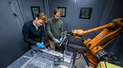
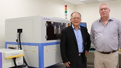
Image – Left: TZ6000 System incorporated with TeraPulse Lx; Middle: Steve Hsu, CEO of ACE Solution. Right: Dr. Philip Taday, Head of Application of TeraView.
For more information:
ACE Solution, Co., Ltd.
https://www.acesolution.com.tw/en/index/
TeraView