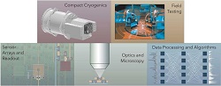
The National Institute of Standards and Technology (NIST) ongoing project will improve time-resolved-emission microscopy (TREM) by tailoring its’ single-photon detectors and scaling up these sensors to the megapixel level.
TREM is a workhorse of semiconductor circuit evaluation. However, as transistor dimensions and power-supply voltages have been reduced, transistor emission has become fainter and signals from multiple transistors are convoluted. The 2023 roadmap from the Electronic Device Failure Analysis Society documents the need for improvements in TREM for circuit analysis of advanced technology nodes. Improving the sensitivity and number of pixels in the sensor arrays are primary objectives for meeting these needs.
When a new integrated circuit is fabricated, it is necessary to measure the chip with microscopy techniques such as photon emission microscopy, which look at infrared photons emitted by electrons accelerated in transistor channels. TREM, also referred to as picosecond imaging circuit analysis, is a variant of this technique that makes use of the temporal information of the emitted photons to precisely determine transistor switching activity in time. With this technique, faint photonic signals generated by transistors are imaged, and the timing information of the photons reveals transistor switching activity. The data from these measurements show which circuit blocks are performing as expected, provide locations of faults, highlight timing errors due to parasitics, and map power consumption.
Two problems have arisen in the past decade: 1) transistors have become much smaller, with 100 transistors located in a diffraction-limited spot, and 2) the power-supply voltage (Vdd) has been reduced to around 0.7 V, which results in much fainter emission shifted into the mid-infrared. Current TREM signal are extremely faint, requiring long integration. Identifying errant transistors has become much more difficult, with signals from 100 transistors impinging on a single sensor.
To overcome these problems, three advances are required:
- More sensitive photon detectors that can receive light at longer wavelengths (2μm);
- Higher-speed sensors so signals from many transistors that cannot be resolved in space can be separated in time; and
- Large arrays of these sensors collecting many channels of data simultaneously, dramatically reducing data acquisition time in a non-destructive manner.
The TREM technique was developed to inform circuit models at all levels of physics from electron transport to SPICE level, providing granular information on signal integrity, reliability, and power consumption. TREM measurements provide this information across all operating temperatures, drive frequencies, and bias conditions. Further a major component of this project will be to develop new AI algorithms to gain further insights from the measured data.
NIST’s approach will enable the disambiguation of authentic chips from counterfeits, identification of the technology node used to manufacture the chip, post-foundry tamper-detection, and possibly the discovery of the entire netlist of an unknown integrated circuit within one day. These insights are highly relevant to hardware security, particularly for critical-path components used in the context of national security, communicated to NIST by IARPA and the Air Force.
Image – Courtesy of: NIST, Jeff Shainline.
For more information:
NIST