Samsung Electronics Co., South Korea, the world’s largest memory chipmaker, plans to unveil an advanced three-dimensional (3D) chip packaging technology to compete with foundry leader Taiwan Semiconductor Manufacturing Company (TSMC).
Samsung will use the technology – SAINT, or Samsung Advanced Interconnection Technology – to integrate memory and processors required of high-performance chips, including AI chips, in much smaller sizes.
Under the SAINT brand, Samsung plans to unveil three types of technologies – SAINT S, which vertically stacks SRAM memory chips and the CPU; SAINT D, which involves vertical packaging of processors such as the CPU and GPU and DRAM memory; and SAINT L, which stacks application processors (APs), people familiar with the matter said on Sunday.
Some of Samsung’s new technologies, including SAINT S, have already passed validation tests. However, Samsung will launch its commercial services next year after further tests with clients, sources said.
The industry’s current mainstream is 2.5D packaging, which places chips horizontally as close together as possible side by side to reduce data bottlenecks. The world’s No. 1 contract chipmaker TSMC is also the leader in the global advanced packaging market with its decade-old 2.5D packaging technology.
Leading chipmakers such as TSMC, Samsung and Intel Corp. are fiercely competing for advanced packaging, which integrates different semiconductors or vertically interconnects multiple chips. Advanced packaging allows multiple devices to be merged and packaged as a single electronic device. The technology has been rapidly increasing in line with growth in generative AI such as ChatGPT, which requires semiconductors that can process large data quickly.
TSMC is spending heavily to test and upgrade its 3D inter-chip stacking tech, SoIC, for its clients, including Apple Inc. and Nvidia Corp. TSMC said in July it will invest 90 billion Taiwanese dollars ($2.9 billion) in a new domestic advanced packaging plant.
Earlier this month, Taiwan’s United Microelectronics Corp. (UMC), the world’s No. 3 foundry player, launched its wafer-to-wafer (W2W) 3D IC project to provide its clients with cutting-edge solutions for efficiently integrating memory and processors using silicon stacking technology.
UMC said its W2W 3D IC project, in collaboration with packaging firms such as ASE, Winbond, Faraday, and Cadence Design Systems, is an ambitious undertaking that seeks to leverage 3D chip integration technology to address the specific requirements of edge AI applications.
Intel uses its next-generation 3D chip packaging tech, Foveros, to make advanced chips.
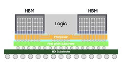
Samsung, the world’s No. 2 foundry company, has been accelerating the development of its chip packaging technology since it unveiled its 2.5D packaging technology H-Cube in 2021. This tech allows logic chips or high-bandwidth memory (HBM) to be stacked on top of a silicon interposer in a small form factor, Samsung said.
The Korean company said in April it is offering a packaging turnkey service, handling the entire process from chip production to packaging and tests.
With its new SAINT technology, Samsung aims to improve the performance of AI chips for data centers and mobile APs with on-device AI functions, sources said.
Image – Samsung’s 2.5D H-Cube chip packaging solution.
For more information:
Samsung Electronics Co.