


Milestone for light-driven electronics: excitons generated in a topological insulator for the first time

An international team of scientists collaborating within the Würzburg-Dresden Cluster of Excellence ct.qmat, Germany, has achieved a breakthrough in quantum research – the first detection of excitons (electrically neutral quasiparticles) in a topological insulator. This discovery paves the way for a new generation of light-driven computer chips and quantum technologies. It was enabled thanks to smart material design in Würzburg, the birthplace of topological insulators. The findings have been published in the journal Nature Communications.

In their search for novel materials for future quantum technologies, scientists from the Cluster of Excellence ct.qmat – Complexity and Topology in Quantum Matter – at the two universities in Würzburg and Dresden are concentrating on topological insulators, which enable the lossless conduction of electrical current and robust information storage. The first experimental realization of this materials class took place in Würzburg in 2007, prompting a worldwide research boom in solid-state physics that continues to this day.

Previous concepts for using topological insulators are based on the application of electrical voltages in order to control currents – an approach adopted from conventional computer chips. However, if the exotic material properties are based on electrically neutral particles (which are neither positively nor negatively charged), an electric voltage no longer works. Such quantum phenomena therefore require other tools if they are to be generated at all – for example, light.

An international research team headed by Professor Ralph Claessen, quantum physicist from Würzburg and co-spokesperson of ct.qmat, has now made a crucial discovery. “For the first time, we’ve been able to generate and experimentally detect quasiparticles known as excitons in a topological insulator. We’ve thus created a new toolkit for solid-state physics that can be used to control electrons optically.” As Claessen emphasizes, “This principle could become the basis for a new type of electronic components.”

Excitons are electronic quasiparticles. Although they seem to behave like independent particles, they actually represent an excited electronic state that can only be generated in certain types of quantum matter. “We created excitons by applying a short light pulse to a thin film consisting of just one single layer of atoms,” explains Claessen. What’s unusual about this, he says, is that the excitons were activated in a topological insulator – something that wasn’t possible before. “This has opened up a completely new line of research for topological insulators,” adds Claessen.

The right starting material is crucial – in this case bismuthene. “It’s the heavy sibling of the miracle material graphene,” says Claessen, who first tailored the topological insulator in the lab five years ago. “We’re the global leaders in this field,” he adds. “Due to our sophisticated materials design, the atoms of the single layer of bismuthene are arranged in a honeycomb pattern, just like graphene. The difference is that bismuthene’s heavy atoms make it a topological insulator, meaning it can conduct electricity along the edge without loss – even at room temperature. This can’t be done by graphene.”

For about ten years, excitons have been investigated in other two-dimensional semiconductors and regarded as information carriers for light-driven components. “For the first time, we’ve managed to optically excite excitons in a topological insulator. The interaction between light and excitons means we can expect new phenomena in such materials. This principle could be used, for example, to generate qubits,” says Claessen.

Qubits are computing units for quantum chips. They’re far superior to traditional bits and allow to solve tasks within minutes for which conventional supercomputers would literally take years.i Using light instead of electrical voltage enables quantum chips with much faster processing speeds. The latest findings therefore pave the way for future quantum technologies and a new generation of light-driven devices in microelectronics.

Image – Three excitons (pairs consisting of an electron and an electron hole) on the topological insulator bismuthene. Due to the honeycomb atomic structure, electrons can only flow along the edges. This topological effect allows current to flow without resistance. Researchers from ct.qmat have managed to generate excitons in a topological insulator for the very first time, paving the way for novel light-driven components – and possibly even the realization of qubits. Courtesy of Jörg Bandmann/ct.qmat.


For more information:

Würzburg-Dresden Cluster of Excellence ct.qmat
https://www.ctqmat.de/en


Imec enables tight standard cell boundary scaling using a two-level semi-damascene integration scheme

Imec, Belgium, a world-leading research and innovation hub in nanoelectronics and digital technologies, presents a semi-damascene integration approach for implementing the vertical-horizontal-vertical (VHV) scaling booster – intended to enable 4-track (4T) standard cells. The semi-damascene process enables cell boundary scaling down to 8nm tip-to-tip (T2T) in the middle-of-line (MOL) layers, providing self-aligned edges.

This provides a booster that designers can use for packing standard cells tighter, representing a 21 percent area gain over 5T designs. The novel routing scheme, along with the semi-damascene integration approach, will be critical to gradually push the logic scaling roadmap well into the Å era.

For a long time, the MOL, which provides the connection between the front-end-of-line (FEOL) and back-end-of-line (BEOL), has been organized as a single-layer contact. But currently, it is expanding into several layers, including, for example, the Mint and Vint layers. These MOL layers carry the electrical signals from the transistor’s source, drain, and gate to the local interconnects and vice versa.

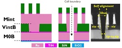
Imec recently introduced a novel standard cell routing architecture called VHV, which involves the introduction of an extra MOL layer (M0B) as a scaling booster to enable 4T standard cell designs. With this booster, the first three routing layers in the standard cell follow a VHV routing style instead of the traditional HVH routing style in 5T standard cells. However, the novel two-level MOL VHV scaling booster is challenging from a process integration point of view, mainly arising from the tight boundary between neighboring 4T standard cells. The cell boundary requires a tight T2T between adjacent MOL M0B lines and two vias (VintB) facing each other with well-defined via edges – all at a minimum distance of one critical dimension (CD) of the top Mint layer. This means that the T2T and VintB via distance will need to be gradually reduced from ~24nm to ~8nm for upcoming technology nodes. This can no longer be achieved using a direct lithographic print but requires a self-aligned patterning strategy instead.

Researchers defined the tight boundary between adjacent standard cells using a two-level semi-damascene approach involving a direct metal etch. Zsolt Tőkei, program director of nano-interconnects and fellow at imec said, “Roughly speaking, we start from conventionally defined continuous lines and wider vias and, once two metal layers are finished, we split them into two, using the top 16-18nm pitch Mint layer as a hard mask for the final patterning step. This results in 3 edges (of Mint, VintB, and M0B) that are simultaneously self-aligned. With our Ru-based two-level test vehicle, we obtained an average via CD of 10.5nm and M0B T2T as tight as 8.9nm – a key achievement.” Imec researchers complemented structural validation with an initial electrical characterization of line resistance and isolation properties.

“The VHV routing scheme is a critical scaling booster to enable cell boundaries at the A10, A7, A5, A3 technology nodes,” adds Tőkei. “It also applies to future device architectures such as nanosheet, forksheet, and CFET. By extending semi-damascene from the BEOL towards the MOL, we have now also found a way to integrate this promising booster. More detailed investigations will, however, be needed, and for that purpose, imec is taping out a new dedicated mask.”


Image – (Left/middle) Schematic representation of the semi-damascene process flow used to test the key features of VHV. (Right) TEM image of the test vehicle after the final Ru etch: T2T M0B and VintB via are self-aligned to the 18mn pitch Mint layer.


For more information:

Imec

www.imec-int.com


Applied Materials launches ‘Singapore 2030’ plan to expand its operations and innovation capabilities

Applied Materials, Inc., Santa Clara, Calif., announced “Singapore 2030” – a multi-faceted plan to expand its operations in Singapore over the next eight years. The plan is targeted at strengthening the company’s global manufacturing and R&D capabilities, broadening technology ecosystem partnerships in Singapore and promoting local workforce development.

“For the past 30 years, Singapore has been a strategic hub for Applied Materials, and we are excited to build on our success with new investments that will strengthen our ability to support the semiconductor industry on its path to becoming a US$1 trillion market by the end of the decade,” said Gary Dickerson, president and CEO of Applied Materials. “We look forward to working with the Government of Singapore and the vibrant technology ecosystem to create opportunities for mutual growth that will benefit the global semiconductor industry.”

With the semiconductor industry entering a new wave of growth fueled by digital transformation of the economy, Applied has announced its intention to make multi-billion-dollar investments in its innovation infrastructure in the United States and to expand its global manufacturing capacity. As part of Singapore 2030, Applied Materials held a groundbreaking ceremony for an expansion of its regional hub in Singapore, which is home to Applied’s largest factory outside of the United States. This investment of hundreds of millions of U.S. dollars will strengthen the company’s ability to meet growing customer demand in the years ahead.

In addition, the company will invest to bolster its R&D capabilities in Singapore with a focus on accelerating commercialization of new technologies and services that improve chip power, performance, area, cost and time-to-market (PPACt). One example is the research collaboration between Applied and the Institute of Microelectronics (IME), a research institute of Singapore’s Agency for Science, Technology and Research (A*STAR), focused on hybrid bonding and other emerging, 3D chip integration technologies.

As a top employer, Applied will help enable a future-ready workforce for Singapore’s semiconductor equipment industry through enhanced training and advanced education programs. This includes an initiative with the Singapore Institute of Technology where Applied employees gain access to tailored learning modules in areas including AI and machine learning, smart manufacturing, robotics and automation, data science, and more.

Applied Materials established its presence in Singapore in 1991 with a small sales and service site that has grown to become a major manufacturing and regional operations hub with a workforce of more than 2,500. In 2019, Applied received the Distinguished Partner in Progress Award from the Government of Singapore in recognition of the company’s outstanding contributions and commitment to the country.


For more information:

Applied Materials, Inc.

www.appliedmaterials.com


Blocking radio waves and electromagnetic interference with the flip of a switch

Researchers in Drexel University’s College of Engineering have developed a thin film device fabricated by spray coating that can block electromagnetic radiation with the flip of a switch. The breakthrough, enabled by versatile two-dimensional materials called MXenes, could adjust the performance of electronic devices, strengthen wireless connections, and secure mobile communications against intrusion.
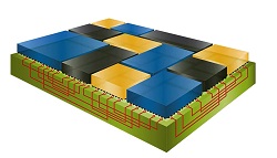
The team previously demonstrated that two-dimensional layered MXene materials – discovered just over a decade ago – when combined with an electrolyte solution, can be turned into a potent active shield against electromagnetic waves. This latest MXene discovery, reported in Nature Nanotechnology, shows how this shielding can be tuned when a small voltage – less than that produced by an alkaline battery – is applied.

MXene is a unique material in that it is highly conductive making it perfectly suited for reflecting microwave radiation that could cause static, feedback, or diminish the performance of communications devices. But its internal chemical structure can also be temporarily altered to allow these electromagnetic waves to pass through.

This means that a thin coating on a device or electrical components prevents them from both emitting electromagnetic waves, as well as being penetrated by those emitted by other electronics. Eliminating the possibility of interference from both internal and external sources can ensure the performance of the device, but some waves must be allowed to exit and enter when it is being used for communication.

The key to eliciting bidirectional tunability of MXene’s shielding property is using the flow and expulsion of ions to alternately expand and compress the space between material’s layers, like an accordion, as well as to change the surface chemistry of MXenes.

With a small voltage applied to the film, ions enter – or intercalate – between the MXene layers altering the charge of their surface and inducing electrostatic attraction, which serves to change the layer spacing, the conductivity and shielding efficiency of the material. When the ions are deintercalated as the current is switched off, the MXene layers return to their original state.

The team tested 10 different MXene-electrolyte combinations, applying each via paint sprayer in a layer about 30 to 100 times thinner than a human hair. The materials consistently demonstrated the dynamic tunability of shielding efficiency in blocking microwave radiation, which is impossible for traditional metals like copper and steel. And the device sustained the performance through more than 500 charge-discharge cycles.

These results indicate that the MXene films can convert from electromagnetic interference shielding to quasi-electromagnetic wave transmission by electrochemical oxidation of MXenes. The MXene film can potentially serve as a dynamic EMI shielding switch.
For security applications, the team suggests that the MXene shielding could hide devices from detection by radar or other tracing systems. The team also tested the potential of a one-way shielding switch. This would allow a device to remain undetectable and protected from unauthorized access until it is deployed for use.

The next step for the team is to explore additional MXene-electrolyte combinations and mechanisms to fine-tune the shielding to achieve a stronger modulation of electromagnetic wave transmission and dynamic adjustment to block radiation at a variety of bandwidths.


For more information:

Drexel University

https://drexel.edu


Chipletz selects Siemens’ EDA solutions for its smart substrate IC packaging technology

Siemens Digital Industries Software, Plano, Texas, announced that Chipletz, an innovative fabless substrate startup, has selected Siemens as its strategic electronic design automation (EDA) provider for the development of its groundbreaking Smart Substrate products.

After an extensive technical evaluation of available solutions, Chipletz selected a suite of Siemens’ industry-leading EDA tools for the design and verification of its Smart Substrate technology, which facilitates the heterogeneous integration of multiple ICs in a single package for critical artificial intelligence workloads, immersive consumer experiences, and high-performance computing.

“The Chipletz vision is to revolutionize semiconductor in-package functionality through the development of advanced packaging technology that bridges the gap between the slowing of Moore’s Law and the rising demand for compute performance,” said Bryan Black, chief executive officer of Chipletz. “Our Smart Substrate designs, now in development, are very demanding. Siemens has demonstrated that they have the ideal technology for our needs.”

To design and verify the heterogeneous integration of multiple ICs into a Smart Substrate based package, Chipletz selected Siemens’ Xpedition Substrate Integrator software, Xpedition Package Designer software, Hyperlynx software and Calibre 3DSTACK software solutions.

“Siemens is honored to be selected by Chipletz as a primary semiconductor packaging design and verification supplier,” said AJ Incorvaia, senior vice president of Electronic Board Systems at Siemens Digital Industries Software. “The Chipletz Smart Substrate technology offers Chipletz customers a robust path to bring multiple ICs, even from different vendors, into a wide range of system-in-package configurations using Siemens’ design tools to deliver a high-performing and cost-effective end-product.”


For more information:

Chipletz

https://chipletz.com/


Siemens Digital Industries Software

https://www.sw.siemens.com/en-US/