Skip to content

Perovskites, a ‘dirt cheap’ alternative to silicon, just got a lot more efficient

A study at the University of Rochester, Rochester, N.Y., suggests perovskites — a family of materials nicknamed for their crystalline structure that have shown extraordinary promise in recent years as a far less expensive, equally efficient replacement for silicon in solar cells and detectors — may become far more efficient.

Researchers typically synthesize perovskites in a wet lab, and then apply the material as a film on a glass substrate and explore various applications. Chunlei Guo, professor of optics at the University of Rochester leading the study reported in Nature Photonics, instead proposes a novel, physics-based approach.

By using a substrate of either a layer of metal or alternating layers of metal and dielectric material—rather than glass—he and his coauthors found they could increase the perovskite’s light conversion efficiency by 250 percent.

“No one else has come to this observation in perovskites,” Guo says. “All of a sudden, we can put a metal platform under a perovskite, utterly changing the interaction of the electrons within the perovskite. Thus, we use a physical method to engineer that interaction.”

Metals are probably the simplest materials in nature, but they can be made to acquire complex functions. The Guo Lab has extensive experience in this direction. The lab has pioneered a range of technologies transforming simple metals to pitch black, superhydrophilic (water-attracting), or superhydrophobic (water-repellent). The enhanced metals have been used for solar energy absorption and water purification in their recent studies.

In this new paper, instead of presenting a way to enhance the metal itself, the Guo Lab demonstrates how to use the metal to enhance the efficiency of pervoskites.

“A piece of metal can do just as much work as complex chemical engineering in a wet lab,” says Guo, adding that the new research may be particularly useful for future solar energy harvesting.”

In a solar cell, photons from sunlight need to interact with and excite electrons, causing the electrons to leave their atomic cores and generating an electrical current, Guo explains. Ideally, the solar cell would use materials that are weak to pull the excited electrons back to the atomic cores and stop the electrical current.

Guo’s lab demonstrated that such recombination could be substantially prevented by combining a perovskite material with either a layer of metal or a metamaterial substrate consisting of alternating layers of silver, a noble metal, and aluminum oxide, a dielectric.
The result was a significant reduction of electron recombination through “a lot of surprising physics,” Guo says. In effect, the metal layer serves as a mirror, which creates reversed images of electron-hole pairs, weakening the ability of the electrons to recombine with the holes.

The lab was able to use a simple detector to observe the resulting 250 percent increase in efficiency of light conversion.
Several challenges must be resolved before perovskites become practical for applications, especially their tendency to degrade relatively quickly. Currently, researchers are racing to find new, more stable perovskite materials.

“As new perovskites emerge, we can then use our physics-based method to further enhance their performance,” Guo says.


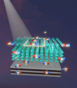
Image – This illustration from the Guo Lab shows the interaction between a perovskite material (cyan) and a substrate of metal-dielectric material. The red and blue pairings are electron-hole pairs. Mirror images reflected from the substrate reduce the ability of excited electrons in the perovskite to recombine with their atomic cores, increasing the efficiency of the perovskite to harvest solar light. Courtesy of: Chloe Zhang.


For more information:

University of Rochester

https://www.rochester.edu/

When quantum computing meets alloy design

Although research alloy design and artificial intelligence has been ongoing for decades, Houlong Zhuang is now combining the two fields to forge a new path forward for materials scientists.
Zhuang’s vision is quickly gaining traction. In fact, the first research article he published about incorporating the use of artificial intelligence to design alloys has already been cited nearly 250 times since 2019.

The National Science Foundation, or NSF, grants the Faculty Early Career Development Program, or CAREER, award to early-career faculty members who have the potential to serve as academic role models in research and education and to lead advances in the mission of their department or organization.

Zhuang has been awarded a $537,000 CAREER award from the NSF to pursue this research in alloy design and quantum computing in his project “Developing Quantum Algorithms for High-Entropy Alloy Discovery.”

Alloy design involves the development of materials made with various metals blended together to create an ideal structural composition. Quantum computing operates by using the subatomic particles in physical matter to store information, then leverages this behavior using specialized hardware. The data drawn from quantum computing can be used to develop methods to mathematically describe the interactions between atoms.

Zhuang’s CAREER award project will build on his work combining alloy design and quantum computing to create quantum algorithms that aid researchers in developing new materials.

These algorithms will be implemented using quantum hardware that produce simulations of the bonds between select elements to predict the best possible combinations of elements to achieve a given material property. Researchers can then conduct experiments to validate if these predictions are correct.

As an assistant professor in the School for Engineering of Matter, Transport and Energy, Zhuang has collaborated with other researchers in the Ira A. Fulton Schools of Engineering and the ASU Quantum Collaborative to use quantum computing to answer questions about atomic interactions in a given chemical composition.

“This project aims to search for a ‘materials genome’ for alloy design using state-of-the-art quantum computers,” Zhuang says. “We are looking forward to identifying promising materials candidates that are suitable for sustainable energy applications like the future hydrogen economy.”

Photo: ASU Assistant Professor Houlong Zhuang has been recognized with a National Science Foundation CAREER award to continue his research at the intersection of alloy design and quantum computing. Photo by Erika Gronek/ASU 

For more information: Arizona State University 

Masan High-Tech Materials integrates global R&D activities under H.C. Starck Tungsten Powders‘ leadership

H.C. Starck Tungsten Powders, Germany, is bringing together the research and development activities within the Masan High-Tech Materials Group in an integrated structure. This will create an international innovation hub with a total of almost 40 highly specialized employees at the headquarters in Goslar and at Masan Tungsten LLC in Thai Nguyen, Vietnam.
The combined team focuses on application research in pyro- and hydrometallurgy, the optimization of existing processes and products, and the development of new, disruptive solutions and technologies.

The combined resources and capabilities are intended to make the company’s innovation processes even more powerful, flexible and effective. To achieve this, further investments in laboratory equipment and qualification measures are planned, especially at the Masan Tungsten LLC, APT Factory in Thai Nguyen.

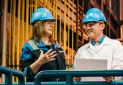
Image – Julia Meese-Marktscheffel, Director Technology and Innovation Global at H.C. Starck Tungsten Powders, with Dai Ngyuen Van, R&D Manager at Masan High-Tech Materials’ Thai Nguyen site.


For more information:

H.C. Starck Tungsten Powders

https://www.hcstarck.com

Spray Tips: Electrolytic fabrication techniques

Electrolytic methods of forming metals that can be electrodeposited are versatile, and it is possible to produce powders of approximately 60 metals. The majority are obtained by molten-salt electrolysis, and powders of approximately 20 metals can be electrodeposited from aqueous solutions. While a larger number of metals can be obtained in powder form by way of molten-salt electrolysis, the larger quantities of powders are produced by electrolysis from aqueous solutions. Powders such as copper, iron, and nickel are obtained from aqueous solutions.

Electrodeposited metal powders are of high purity and therefore are extremely active during sintering. However, they demonstrate the following deficiencies: the process demands purification so that residual impurities could be removed, the electrolysis technique is often expensive, and the process is usually limited to the production of pure metal (i.e., nonalloyed) powders.

Electrolytic metal powder forms as a dendritic electrodeposit, which can spontaneously fall off or can be removed from the electrode by tapping or by other similar ways. The powder has a tendency to form flakes or needles, or be deposited in fibrous or spongy forms, depending on the electrodeposition process parameters and on the nature of the metal.

Electrolysis conditions that favor the diffusion process of electrodeposition enhance the formation of electrolytic metal powder. For example, a decrease of metal salt concentration, an increase in concentration of an electrolyte, a decrease of stirring rate, an increase of current density, a decrease of temperature, and an increase of the solution viscosity are factors favoring powder formation. In addition to these factors, the deposit structure depends on the nature of the metal and the salt species used in the electrolyte solution.

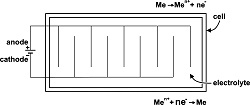
The scheme of an electrolytic cell for electrodeposition of metal powder is shown in the image. It is similar to a cell that is used for electroplating. The cell must have a slanting bottom so that the powder can be guided to a collection place for removal.

Image – Electrolytic cell for the deposition of metal powder.

This information is from ASM Handbooks Online, Vol. 5A: Thermal Spray Technology, Coating Structures, Properties, and Materials. To find this information (subscription required), click on the link below and scroll down to Figure 4.

https://dl.asminternational.org/handbooks/edited-volume/12/chapter/133823/Feedstock-Material-Considerations-for-Thermal


Gatan introduces Cipher, the first tool to determine lithium content quantitatively in the scanning electron microscope

AMETEK Gatan, Inc., Berwyn, PA, a global leader focused on enhancing and extending the operation and productivity of electron microscopes, announced the launch of the Cipher system—the first and only system that reveals, quantitatively, the distribution of lithium in conventional scanning electron microscopes (SEM) and dual beam instruments.

To successfully reach the energy reduction pledges of governments worldwide, researchers are developing lithium compounds and alloys to improve the capacity and storage of renewable energy technologies. Quantifying and understanding the micro-scale distribution of lithium now becomes ever more pressing during the development of this integral technology. Still, the observation of lithium in bulk materials at these length scales has remained tantalizingly out of reach.

“For many years, a method to reliably detect lithium has been considered the ‘holy grail’ of microanalysis. However, due to fundamental limits of physics, reliable measurement of the lithium content in critical materials such as those used in lithium-ion batteries has proved unachievable,” says David Stowe, SEM Product Manager, Gatan/EDAX. “With the launch of Cipher, a ground-breaking method is now available to reveal the lithium content in metallic alloys, compounds, and complex metal oxides down to low single-digit weight percentages.”

Using an original concept, the Cipher system combines quantitative analysis of backscattered electrons and the x-ray fluorescence signal to reveal lithium using a composition-by-difference method. Building on AMETEK’s expertise in detector technologies, researchers can now utilize a turnkey solution in the DigitalMicrograph software to collect quantitative data, correlate, and analyze lithium at the micro-scale.

“With this release of the Cipher system, we see the accelerated innovation that was foreseen by bringing the EDAX and Gatan brands together,” commented Narayan Vishwanathan, vice president and business unit manager of AMETEK Electron Microscopy Technologies. “We now bring a reliable method to detect lithium that will fast-track the development of improved renewable energy materials.”

For more information:

AMETEK Gatan

https://www.gatan.com/

Electronic bridge allows rapid energy sharing between semiconductors

Researchers at the Department of Energy’s Lawrence Berkeley National Laboratory (Berkeley Lab), Berkeley, Calif., discover that electrons play a surprising role in heat transfer between layers of semiconductors, with implications for next-generation electronic devices.

As semiconductor devices become ever smaller, researchers are exploring two-dimensional (2D) materials for potential applications in transistors and optoelectronics. Controlling the flow of electricity and heat through these materials is key to their functionality, but first we need to understand the details of those behaviors at atomic scales.

Curious about how electrons and atomic vibrations couple to one another when heat flows between two materials, zooming into the interface with atomic precision allowed the researchers to uncover a surprisingly efficient mechanism for their coupling.

“Our work shows that we need to go beyond the analogy of Lego blocks to understand stacks of disparate 2D materials, even though the layers aren’t strongly bonded to one another,” said Archana Raja, a scientist at Berkeley Lab at who led the study. “The seemingly distinct layers, in fact, communicate through shared electronic pathways, allowing us to access and eventually design properties that are greater than the sum of the parts.”

In stacked layers of the 2D semiconductor materials tungsten diselenide (WSe2) and tungsten disulfide (WS2), researchers found that although they aren’t tightly bonded to one another, electrons provide a bridge between them that facilitates rapid heat transfer.

The devices were fabricated by Raja’s group at Berkeley Lab’s Molecular Foundry, who perfected the art of using Scotch tape to lift off crystalline monolayers of the semiconductors, each less than a nanometer in thickness. Using polymer stamps aligned under a home-built stacking microscope, these layers were deposited on top of each other and precisely placed over a microscopic window to enable the transmission of electrons through the sample.

In experiments conducted at the Department of Energy’s SLAC National Accelerator Laboratory, the team used ultrafast electron diffraction (UED) to measure the temperatures of the individual layers while optically exciting electrons in just the WSe2 layer. The UED served as an “electron camera”, capturing the atom positions within each layer. By varying the time interval between the excitation and probing pulses by trillionths of a second, they could track the changing temperature of each layer independently, using theoretical simulations to convert the observed atomic movements into temperatures.

The UED approach enables a new way of directly measuring temperature within this complex heterostructure.  Aaron Lindenberg, a co-author on the study at Stanford University said “These layers are only a few angstroms apart, and yet we can selectively probe their response and, as a result of the time resolution, can probe at fundamental time scales how energy is shared between these structures in a new way.”

They found that the WSe2 layer heated up, as expected, but to their surprise, the WS2 layer also heated up in tandem, suggesting a rapid transfer of heat between layers. By contrast, when they didn’t excite electrons in the WSe2 and heated the heterostructure using a metal contact layer instead, the interface between WSe2 and WS2 transmitted heat very poorly, confirming previous reports.

“It was very surprising to see the two layers heat up almost simultaneously after photoexcitation and it motivated us to zero in on a deeper understanding of what was going on,” said Raja.

To understand their observations, the team employed theoretical calculations, using methods based on density functional theory to model how atoms and electrons behave in these systems with support from the Center for Computational Study of Excited-State Phenomena in Energy Materials (C2SEPEM), a DOE-funded Computational Materials Science Center at Berkeley Lab.

The researchers conducted extensive calculations of the electronic structure of layered 2D WSe2/WS2, as well as the behavior of lattice vibrations within the layers. Like squirrels traversing a forest canopy, who can run along paths defined by branches and occasionally jump between them, electrons in a material are limited to specific states and transitions (known as scattering), and knowledge of that electronic structure provides a guide to interpreting the experimental results.

Using computer simulations, the team explored where the electron in one layer initially wanted to scatter to, due to lattice vibrations. They found that electrons wanted to scatter to a hybrid state – a kind of ‘glue state’ where the electron hangs out in both layers at the same time. Now the team has a good idea of what these glue states look like and their signatures to confidently say that other, 2D semiconductor heterostructures will behave the same way.

The study appeared recently in Nature Nanotechnology.


Image – Artistic depiction of electron transfer driven by an ultrashort laser pulse across an interface between two atomically-thin materials. This transfer is facilitated by an interlayer ‘bridge’ state that electrons are able to access due to lattice vibrations in both materials. Courtesy of: Gregory M. Stewart/SLAC.


For more information:

Lawrence Berkeley National Laboratory

https://www.lbl.gov/

U.S. Department of Energy’s Office of Science

https://www.energy.gov/science/office-science

One Minute Mentor: Fluidized-bed heat treating furnace

The indirectly heated fluidized-bed furnace is heated electrically though a fluidized-bed furnace may also be gas heated. Fluidized beds have been designed to perform a wide variety of heat treating tasks including stress relieving, preheating, hardening, quenching, annealing, and tempering, as well as a variety of surface treatments such as carburizing, nitriding, and steam tempering.

Continue reading

‘Steeling the show’: S&T metallurgists awarded second $2 million grant

A Missouri S&T research team was recently awarded a $2 million grant from the United States Department of Energy to research technologies to improve the operating efficiency of electric arc furnaces (EAFs) used for steelmaking. 
 
“It takes a tremendous amount of power to run an EAF, and we are looking for new ways to lower that energy footprint,” says Dr. Ronald O’Malley, the F. Kenneth Iverson Endowed Chair of Steelmaking Technologies and director of the Kent D. Peaslee Steel Manufacturing Research Center at Missouri S&T. “We are working toward implementing a next-generation dynamic control system for the EAF so we can optimize EAF operating efficiency under changing input conditions using new sensor systems.” 
 
The project is titled “Intelligent Dynamic EAF Advisory System (IDEAS) for Improving EAF Operating Efficiency.” This $2 million grant is part of a larger three-phase project.  
 
For the first phase, the research team assessed the current systems in place at the two steel plants that are partners in the study and developed the conceptual framework for the future aspects of the project. 
 
This stage required significant data analysis for the process, integration of existing control modules already in place, implementation of new control modules and development and testing of new fiber optic sensing technologies in the lab for use in the EAF. 
 
In Phase 2, the new fiber optic sensing technologies will be implemented in the plants along with new control systems, directed energy input and EAF slag property models. 
 
“In basic terms, the fiber optic system will provide a whole new set of tools for EAF optimization,” O’Malley says. “We will be able to better examine the condition of the EAF and the impact of operating variables on the process in real time to provide feedback to the operator and improve energy efficiency, operating cost and yield.” 
 
The new sensor technology and control modules will be installed at the two partner steel plants, which are Big River Steel in Osceola, Arkansas, and Commercial Metals Company (CMC) in Birmingham, Alabama. 
 
After that, the systems will go live, and the data collection process will begin. Throughout the process, the plant employees will be trained on how to use the new technology. Then, in the final stage, the researchers will analyze the performance improvements in progress and determine what changes should be implemented to further improve the system. 
 
“Something people should also appreciate about this project is the benefits to the student researchers involved,” says O’Malley. “S&T and ASU will have a team of undergraduate and graduate students working on this project. You can’t beat the hands-on experience that this will provide for our students.” 
 

For more information: Missouri University of Science and Technology 

Photo: Dr. Ron O’Malley, a professor at Missouri S&T, is leading a study to improve the energy footprint associated with electric arc furnaces. Photo by Michael Pierce/Missouri S&T. 

This smart contact lens could treat glaucoma

Across the world, some 80 million people suffer from glaucoma, a number that’s expected to swell to 111 million by 2040. Today, an estimated three million have been diagnosed in the United States.

But common as it may be, glaucoma is a formidable affliction. It takes root with an accumulation of fluid in the eyes, forming a bubble of extra pressure that slowly damages the optical nerve. At first touch, symptoms can be imperceptible—perhaps a bit of blurriness, or a slight weakening of your peripheral sight. Over time, the angle through which your pupils peer might narrow further and further—until one day, you might wake up with your field of vision completely zeroed out. No cure exists.

Glaucoma can be treated by lowering the extra pressure in the eyes, most often with prescription eye drops. Now, Pohang University of Science and Technology (POSTECH) in South Korea has engineered a way to make the treatment more futuristic, with a smart contact lens that automatically delivers doses of medication over time, straight onto the eyeballs.

The contact lens, developed by a team from POSTECH’s department of materials science and engineering, is fitted with hollow nanowires made of gold, which serve as sensors that constantly track intraocular pressure (IOP). POSTECH’s invention can also administer the appropriate treatment in response to the diagnostic data. It’s powered by an integrated circuit chip, which allows the lens to release amounts of a drug on demand.

Similarly to diabetes, glaucoma is a treatable disease that patients must manage for life. Also, like diabetes, the greatest uphill battle today is adherence. Many patients struggle to remember to check IOP levels, or simply find the monitoring too much of a hassle.

“We hope the early commercialization of the newly developed theranostic smart contact lens for diagnosing and treating glaucoma intraocular pressure [can] provide glaucoma patients’ compliance,” said Sei Kwang Hahn, a POSTECH professor and the study’s lead.

For more information: Nature Communications

Steel corrosion is a major contributor to climate change

Each year, the United States spends almost a trillion dollars trying to combat metallic corrosion, an electrochemical reaction which occurs when metals oxidize and begin to rust. Now, a team of researchers led by the Ohio State University (OSU) has estimated how much corrosion is gradually worsening global carbon emissions.

Although earlier research has already estimated the economic cost of corrosion to be about three to four percent of United States’ gross domestic product, this is the first study to quantify the environmental impact associated with steel corrosion.

Global steel production has increased steadily for decades and, since steel has poor resistance to corrosion, part of that demand is to replace steel from construction materials that have become corroded over time. According to the experts, reducing the amount of steel which needs to be replaced due to corrosion could have significant effects on the amount of greenhouse gases produced to make steel.

“Given society’s reliance on coal fuel, iron and steel production is one of the largest greenhouse gases emitters of any industry. But most of the costs associated with the industry stem from the energy that goes into creating steel, and that energy is lost as the steel reverts to rust, which is like its original form of iron ore,” explained study senior author Gerald Frankel, a professor of Materials Science and Engineering at OSU.

By using historical carbon dioxide intensity data in order to estimate CO2 levels per year starting from 1960, the scientists found that, in 2021, steel production accounted for 27 percent of the carbon emissions of the global manufacturing sector, and approximately 10.5 percent of the total carbon emissions worldwide, while corroded steel emissions accounted for about 1.6 to 3.4 percent of emissions.

Fortunately, due to regulations placed on the steel industry, technological advancements in the steel industry have resulted in a 61 percent reduction in energy consumption over the past half a century. Nonetheless, policy makers and industry officials should still act urgently to amend and coordinate international policy concerning steel production and corrosion management.

“Coordinated international strategies, as well as decreasing global steel demand, by using best practices for corrosion mitigation, could better improve global corrosion management strategies and drastically reduce the rise in greenhouse gas emissions we’re seeing due to repeatedly replacing corroded steel,” Frankel said.

If such actions are not undertaken soon, greenhouse emissions caused by the steel industry could spike to 27.5 percent of the global carbon emissions by as early as 2030, with corroded steel representing four to nine percent of that number. This could have dire impacts on the Earth’s climate.

“Global warming is a societal challenge that takes coordination of a lot of multidisciplinary approaches. Our work is bringing to light an issue that seems to have gone under the radar in terms of the importance of adding to the problem,” Frankel concluded.

For more information: npj Materials Degradation

‘Steeling the show’: S&T metallurgists awarded second $2 million grant

A Missouri S&T research team was recently awarded a $2 million grant from the United States Department of Energy to research technologies to improve the operating efficiency of electric arc furnaces (EAFs) used for steelmaking. 
 
“It takes a tremendous amount of power to run an EAF, and we are looking for new ways to lower that energy footprint,” says Dr. Ronald O’Malley, the F. Kenneth Iverson Endowed Chair of Steelmaking Technologies and director of the Kent D. Peaslee Steel Manufacturing Research Center at Missouri S&T. “We are working toward implementing a next-generation dynamic control system for the EAF so we can optimize EAF operating efficiency under changing input conditions using new sensor systems.” 
 
The project is titled “Intelligent Dynamic EAF Advisory System (IDEAS) for Improving EAF Operating Efficiency.” This $2 million grant is part of a larger three-phase project.  
 
For the first phase, the research team assessed the current systems in place at the two steel plants that are partners in the study and developed the conceptual framework for the future aspects of the project. 
 
This stage required significant data analysis for the process, integration of existing control modules already in place, implementation of new control modules and development and testing of new fiber optic sensing technologies in the lab for use in the EAF. 
 
In Phase 2, the new fiber optic sensing technologies will be implemented in the plants along with new control systems, directed energy input and EAF slag property models. 
 
“In basic terms, the fiber optic system will provide a whole new set of tools for EAF optimization,” O’Malley says. “We will be able to better examine the condition of the EAF and the impact of operating variables on the process in real time to provide feedback to the operator and improve energy efficiency, operating cost and yield.” 
 
The new sensor technology and control modules will be installed at the two partner steel plants, which are Big River Steel in Osceola, Arkansas, and Commercial Metals Company (CMC) in Birmingham, Alabama. 
 
After that, the systems will go live, and the data collection process will begin. Throughout the process, the plant employees will be trained on how to use the new technology. Then, in the final stage, the researchers will analyze the performance improvements in progress and determine what changes should be implemented to further improve the system. 
 
“Something people should also appreciate about this project is the benefits to the student researchers involved,” says O’Malley. “S&T and ASU will have a team of undergraduate and graduate students working on this project. You can’t beat the hands-on experience that this will provide for our students.” 
 

For more information: Missouri University of Science and Technology 

Photo: Dr. Ron O’Malley, a professor at Missouri S&T, is leading a study to improve the energy footprint associated with electric arc furnaces. Photo by Michael Pierce/Missouri S&T. 

Curtiss-Wright acquires Keronite Group

Curtiss-Wright Corp., Davidson, N.C., completed the acquisition of the stock of Keronite Group Limited, U.K., a leading provider of plasma electrolytic oxidation surface treatment applications, for $35 million in cash.

Continue reading

Engineers develop a new kind of shape-memory material

Massachusetts Institute of Technology, Boston, MA, has announced the discovery of a new category of shape-memory materials that could open up a new range of applications, especially for high-temperature settings, such as actuators inside a jet engine or a deep borehole.
Shape-memory metals have long been used as simple actuators in a variety of devices but are limited by the achievable service temperatures of the metals used, usually a few hundred degrees Celsius at most. Ceramics can withstand much higher temperatures, sometimes up to thousands of degrees, but are known for their brittleness. Now, the MIT team has found a way to overcome that and produce a ceramic material that can actuate without accumulating damage, thus making it possible for it to function reliably as a shape-memory material through many cycles of use.


Read further here: https://news.mit.edu/2022/shape-memory-material-ceramic-1005


Surprising speed-dependent friction with graphene

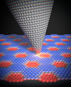
The speed at which an atomic force microscope moves across the surface of certain materials is influenced by the frictional properties of the substrate. One such example is graphene, which consists of a single layer of carbon atoms in a honeycomb arrangement. It is being examined with a view to potential use as a lubricating layer. Applications where a reduction of friction is desired include hard disks or moving components for satellites or space telescopes.

Previous studies have shown that a graphene ribbon can be moved across a gold surface with almost no friction. But if graphene is applied to a platinum surface, it has a significant impact on the measurable friction forces. Now, physicists from the University of Basel and Tel Aviv University have reported in the journal Nano Letters (“Velocity Dependence of Moiré Friction”) that, in this instance, the friction depends on the speed at which the tip of an atomic force microscope (AFM) is moved across the surface.

This finding is surprising because friction does not depend on speed according to Coulomb’s law, which applies in the macro world.

In conjunction with the platinum substrate, graphene no longer forms only the hexagonal honeycomb pattern of carbon atoms and instead forms superstructures known as Moiré superlattices. The surface is then no longer completely flat and exhibits a certain degree of roughness.

“If we move the AFM tip across this slightly corrugated surface at low speed, we measure a weak and almost constant frictional force,” explains Professor Ernst Meyer from the Swiss Nanoscience Institute and the Department of Physics at Basel University. “Above a certain threshold, however, the friction then increases with the speed of the AFM tip,” adds first author Dr. Yiming Song. “The larger the Moiré superstructure, the lower the threshold at which the friction becomes speed-dependent.”

The researchers found that there is greater resistance at the ridges of the Moiré superstructures during the movement of the tip. These ridges undergo elastic deformation due to the pushing tip before relaxing again when the pressure is sufficiently high. This effect results in greater frictional forces that increase with the speed of the tip. Simulations and an analytical model confirm the experimental findings obtained by this international team of researchers.

Image – The friction between the tip of an atomic force microscope and the Moiré superstructures depends on the speed at which the tip is moved across the surface. Courtesy of University of Basel.

************

For more information:

University of Basel

Johnson Matthey and BP produces product for Fulcrum’s Sierra waste-to-fuels plant

Johnson Matthey, UK, has announced that their technology has enabled Fulcrum’s Sierra BioFuels Plant to successfully produce synthetic crude oil for clean transportation fuels.
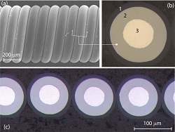
Using Johnson Matthey (JM) and BP’s FT CANS technology, the Sierra plant is the world’s first commercial-scale plant to use household rubbish as a feedstock that would otherwise be destined for landfill. The plant will produce synthetic crude oil, which is expected to ultimately be refined to approximately 11 million gallons of renewable, low-carbon transportation fuels each year from approximately 175,000 tons of landfill waste. JM and bp signed their first license with waste-to-fuels developer Fulcrum to use their award-winning FT CANS technology in 2018.

Read further here.


Superelastic conductor material with enhanced fatigue durability for implantable lead service

Fort Wayne Metals, Ind., has developed a new patent-pending technology to enhance the fatigue life of biostimulation leads.

 

These are used in devices like pacemakers, implantable cardioverter defibrillators, deep brain stimulators, and spinal cord and peripheral nerve stimulators under development in Fort Wayne Metals R&D. Conventional leads employ a composite DFT wire with a 35N LT alloy shell and a conductive silver core. By replacing the 35N LT alloy with superelastic or shape memory nitinol, dramatic improvements in strain-fatigue (and presumably service life) can be achieved. A polyimide coating is further applied to the wire, and with proper care can withstand the shape-setting head treatments needed to form nitinol into the desired lead components like cables and coil.


Read further here: https://www.fwmetals.com/services/r-d/rd-update/


Milestone for light-driven electronics: excitons generated in a topological insulator for the first time

An international team of scientists collaborating within the Würzburg-Dresden Cluster of Excellence ct.qmat, Germany, has achieved a breakthrough in quantum research – the first detection of excitons (electrically neutral quasiparticles) in a topological insulator. This discovery paves the way for a new generation of light-driven computer chips and quantum technologies. It was enabled thanks to smart material design in Würzburg, the birthplace of topological insulators. The findings have been published in the journal Nature Communications.
In their search for novel materials for future quantum technologies, scientists from the Cluster of Excellence ct.qmat – Complexity and Topology in Quantum Matter – at the two universities in Würzburg and Dresden are concentrating on topological insulators, which enable the lossless conduction of electrical current and robust information storage. The first experimental realization of this materials class took place in Würzburg in 2007, prompting a worldwide research boom in solid-state physics that continues to this day.

Previous concepts for using topological insulators are based on the application of electrical voltages in order to control currents – an approach adopted from conventional computer chips. However, if the exotic material properties are based on electrically neutral particles (which are neither positively nor negatively charged), an electric voltage no longer works. Such quantum phenomena therefore require other tools if they are to be generated at all – for example, light.

An international research team headed by Professor Ralph Claessen, quantum physicist from Würzburg and co-spokesperson of ct.qmat, has now made a crucial discovery. “For the first time, we’ve been able to generate and experimentally detect quasiparticles known as excitons in a topological insulator. We’ve thus created a new toolkit for solid-state physics that can be used to control electrons optically.” As Claessen emphasizes, “This principle could become the basis for a new type of electronic components.”

Excitons are electronic quasiparticles. Although they seem to behave like independent particles, they actually represent an excited electronic state that can only be generated in certain types of quantum matter. “We created excitons by applying a short light pulse to a thin film consisting of just one single layer of atoms,” explains Claessen. What’s unusual about this, he says, is that the excitons were activated in a topological insulator – something that wasn’t possible before. “This has opened up a completely new line of research for topological insulators,” adds Claessen.

The right starting material is crucial – in this case bismuthene. “It’s the heavy sibling of the miracle material graphene,” says Claessen, who first tailored the topological insulator in the lab five years ago. “We’re the global leaders in this field,” he adds. “Due to our sophisticated materials design, the atoms of the single layer of bismuthene are arranged in a honeycomb pattern, just like graphene. The difference is that bismuthene’s heavy atoms make it a topological insulator, meaning it can conduct electricity along the edge without loss – even at room temperature. This can’t be done by graphene.”

For about ten years, excitons have been investigated in other two-dimensional semiconductors and regarded as information carriers for light-driven components. “For the first time, we’ve managed to optically excite excitons in a topological insulator. The interaction between light and excitons means we can expect new phenomena in such materials. This principle could be used, for example, to generate qubits,” says Claessen.

Qubits are computing units for quantum chips. They’re far superior to traditional bits and allow to solve tasks within minutes for which conventional supercomputers would literally take years.i Using light instead of electrical voltage enables quantum chips with much faster processing speeds. The latest findings therefore pave the way for future quantum technologies and a new generation of light-driven devices in microelectronics.

Image – Three excitons (pairs consisting of an electron and an electron hole) on the topological insulator bismuthene. Due to the honeycomb atomic structure, electrons can only flow along the edges. This topological effect allows current to flow without resistance. Researchers from ct.qmat have managed to generate excitons in a topological insulator for the very first time, paving the way for novel light-driven components – and possibly even the realization of qubits. Courtesy of Jörg Bandmann/ct.qmat.


For more information:

Würzburg-Dresden Cluster of Excellence ct.qmat

https://www.ctqmat.de/en


Unlikely union of 3D-printed bronze and steel holds promise for jet engines

Skoltech researchers have used a 3D printer to fabricate samples of bronze-steel alloys previously unknown to materials science and investigated their mechanical characteristics. Blending the distinct properties of bronze and steel, the novel alloys could be used to manufacture combustion chambers for aircraft and rocket engines that would simultaneously benefit from steel’s ability to withstand extreme temperatures and bronze’s capacity to conduct heat away from the chamber and thus prevent the engine from overheating.

“3D printing is promising for manufacturing composite parts, endowed with the properties of the two distinct materials that make up the composite,” Associate Professor Igor Shishkovsky of Skoltech Materials explained. “Consider, for example, that steel is resistant to the high temperatures created by fuel combustion in an operating engine. This is great, but compared with bronze, steel is a modest thermal conductor, so the engine coolant cannot siphon heat away from it as effectively to prevent overheating and damage. Well, with 3D printing, you can actually get the best of both worlds by manufacturing a combustion chamber that seamlessly goes from being bronze on the inside for better temperature management to being steel on the outside for holding the structure together.”

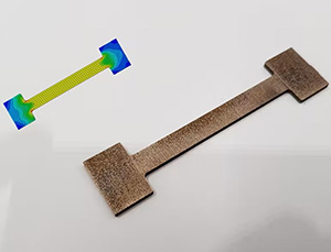
Shishkovsky was the principal investigator on the study that reported the first-ever synthesis of a bronze-steel alloy using a 3D printing technique called direct laser deposition, which melts and fuses powdered ingredients by a laser beam at every successive point in the metal part just as it’s being created. In fact, the Skoltech team combined bronze and steel in two different ways, obtaining both so-called quasi-homogeneous alloys and sandwich structures. In the former, the two materials are more or less evenly intermixed throughout the sample, while the latter consists of a series of alternating 0.25-millimeter-thick layers of bronze and steel. The researchers used one type of steel but varied its content in the alloy from 25% to 50% and experimented with three different common varieties of bronze.

The study confirmed that the two materials fused well, without defects forming, and investigated the bronze-steel alloy’s structural and mechanical properties. To do this, the team grew vertical bars from the bottom up and examined their shape, chemical composition, and microstructure.

Finding no problems at this stage, the researchers proceeded to cut out tiny pieces from different parts of the samples and investigated their internal structure with optical and scanning electron microscopy. The main mechanical characteristics were then obtained in a wide range of mechanical tests of sandwich composites continued up to their destruction. These properties are reported for the first time.

The study’s first author Konstantin Makarenko, a fourth-year Ph.D. student at Skoltech Materials, said, “Now that we have confirmed that steel and bronze can be combined in an alloy and are compatible with 3D printing via direct laser deposition, and we know the mechanical characteristics of the new material, we can explore its possible applications.  Looking forward, I would like to manufacture and test a steel-bronze combustion chamber at Skoltech, but beyond that, other items are possible and other metal combinations could be used. The next step would be to create turbine blades made of a strengthened superalloy with cooling channels made of bronze. It’s all about combining the benefits of two distinct materials in one seamless product without any welding or other junctures.”

For more information: Materials & Design

SMA Actuator Design Tools for the Experienced and the Rookie Users

The primary goal of the Consortium for the Advancement of Shape Memory Alloy Research and Technology (CASMART) is to enable the design of revolutionary applications based on shape memory alloy (SMA) technology. Currently, one of the major roadblocks for the integration of SMA-based actuation systems is the development cost. Therefore, the Design Working Group of CASMART has developed SMA actuator design tools for three common actuator types: wires, springs, and torque tubes.

Continue reading

One Minute Mentor: Fluidized-Bed Furnace

A fluid bed results when a gas is passed upward through a bed of small solid particles at a rate fast enough to lift these particles and to create turbulence. This motion of particles, which are usually made of aluminum oxide or silica oxide, is similar to that of a fluid.

Continue reading

Bodycote to offer new services in the Middle East

Bodycote, the world’s largest provider of heat treatment and specialist thermal processing services, is expanding its thermal spray coatings capability in the Middle East. Bodycote has entered into a partnership with Mathevon Group to develop the market in the region and, in particular, Saudi Arabia

Continue reading