Layered assembly of 2D materials such as graphene has potential roles in the development of new electronic devices. Manufacturing these materials at a large scale while making them atomically clean is a major challenge. This new cleaning mechanism is an important tool. It will help researchers develop manufacturing protocols for large area, high-quality devices. It will also streamline the production of these materials by removing the need for additional processes after they are cleaned.
Researchers from New York University and the Center for Functional Nanomaterials (CFN), a Department of Energy Office of Science user facility at Brookhaven National Laboratory, used the CFN Quantum Material Press (QPress) to assemble 2D graphene heterostructures materials. This study showed that the interface cleaning process of layered heterostructures made from contaminated 2D layers involves more complex mechanisms than a simple thermal actuation that is typically used to make clean interfaces. The combination of non-bonding interactions of the polymer with graphene, thermally activated mobilization of polymer residues, and mechanical actuation is essential for fabricating heterostructures with atomically clean interfaces from polyvinyl acetate-contaminated graphene. This study opened a new opportunity to develop a more effective process to make large and clean layered heterostructure devices.
For more information: Small
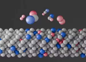
Image: Robotic stacking of 2D material layers on a heated substrate while applying pressure pushes out residues such as polymers from between the layers, resulting in atomically clean interfaces between layers.