Researchers at Intel Foundry have demonstrated a first-of-its-kind GaN chiplet technology built on 300 mm GaN-on-silicon wafers, marking a significant leap forward in semiconductor design. This work tackles one of the most pressing challenges in modern computing: how to deliver more power, speed, and efficiency in an increasingly compact space.
To meet the demand of graphics processors, servers, and wireless networks for ever-greater performance, the Intel Foundry team developed an ultra-thin GaN chiplet — its base silicon measuring just 19 μm thick, roughly one-fifth the width of a human hair — along with the industry’s first fully monolithic on-die digital control circuits, all built using a single integrated manufacturing process.
This technology opens the door to concrete improvements across several industries. In data centers, GaN chiplets could switch faster, losing less energy than silicon alternatives. This would enable voltage regulators that are smaller, more efficient, and positioned closer to the processor — reducing the resistive energy losses that occur over long power routing paths. In wireless infrastructure, the high-frequency performance of GaN transistors makes it a natural candidate for radio frequency (RF) frontend technology such as base stations used in 5G and 6G systems being developed for the next decade. GaN’s ability to operate efficiently at frequencies exceeding 200 GHz positions it well for the centimeter- and millimeter-wave bands on which next-generation networks will rely. Beyond networks, the same capabilities are relevant to radar systems, satellite communications, and photonic applications where fast electrical switching is needed to modulate light signals.
Intel Foundry’s approach — growing GaN on large silicon wafers at the industry-standard 300 mm diameter — allows GaN chiplets to be made using much of the same infrastructure already built for conventional silicon, potentially reducing cost dramatically and enabling the high-volume production the industry requires.
Thinning a semiconductor wafer sounds straightforward, but doing it on a fully processed 300 mm GaN-on-silicon wafer — one that already contains all the transistors and metal wiring layers — without damaging those structures is a formidable engineering challenge. The Intel Foundry team accomplished this using a technique called stealth dicing before grinding (SDBG), which uses a precisely controlled laser to create microscopic fracture lines inside the wafer before a mechanical grinding step reduces its thickness. The result is a GaN chiplet with an underlying silicon base of just 19 μm.
To verify that thinning the wafer did not compromise performance, the team measured the electrical characteristics of transistors on the harvested chiplets. Transistors with gate lengths as short as 30 nanometers (nm) demonstrated excellent current carrying capability, low energy loss, and the ability to block voltages up to 78 volts. The RF performance was equally strong, with transistors achieving operating cut-off frequencies exceeding 300 GHz — well into the range needed for next-generation wireless communications.
Perhaps the most novel aspect of this work is the demonstration of fully functional digital circuits built directly onto the GaN chiplet itself. In conventional electronics, digital control logic — the circuitry that tells a power transistor when to switch on and off — is typically handled by a separate silicon chip.
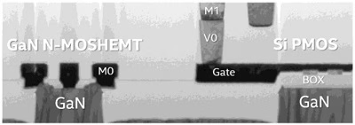
In a chiplet-based system, that separate chip takes up precious space and introduces inefficiencies from the longer electrical pathways between components. The Intel Foundry team offers a potential solution to solve this by combining two types of transistors on the same chiplet: GaN N-channel metal-oxide-semiconductor high-electron-mobility transistors (N-MOSHEMT), which excel at handling power (high voltages), and silicon p-channel metal-oxide-semiconductor field-effect (Si PMOS) transistors, which are well-suited for lower-voltage digital logic. By transferring silicon onto the GaN wafer through a process called layer transfer, both transistor types can be built side-by-side and connected using the same wiring layers.
Using this combined process, the team built and tested a complete library of digital circuit building blocks: inverters (which flip a signal from on to off), NAND gates (a fundamental logic operation), multiplexers (circuits that select between multiple input signals), flip-flops (circuits that store a single bit of information), and ring oscillators (chains of inverters used to measure circuit speed). Every circuit worked correctly, and the speed measurements — with each inverter switching in just 33 picoseconds (ps) or 33 trillionths of a second — were consistent across the entire 300 mm wafer, confirming that the process is uniform and potentially manufacturable at scale.
Demonstrating that a new semiconductor technology works in the lab is only half the battle. Before any chiplet technology reaches real products, it must prove it can operate reliably for years under the stresses of real-world use — heat, high voltages, and sustained electrical current. The Intel Foundry team subjected the GaN transistors to four industry-standard reliability tests, each designed to simulate a different type of stress that chiplets encounter over their lifetime. Promising results in time-dependent dielectric breakdown (TDDB), positive bias temperature instability (pBTI), high-temperature reverse bias (HTRB), and hot-carrier injection (HCI) studies indicate that the 300 mm GaN MOSHEMT technology can meet required reliability metrics.
Image – A cross-sectional electron microscope image showing a GaN power transistor and a silicon logic transistor built side-by-side on the same 300 mm GaN-on-silicon wafer.
For more information:
Intel
https://www.intel.com/