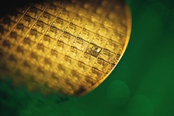
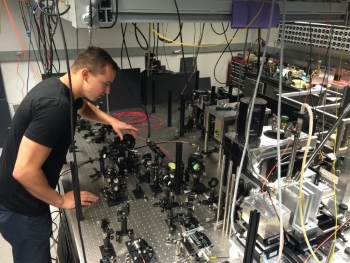
The Agency for Science, Technology, and Research (A-Star), Singapore, reports that a laser-induced thermal cracking technology for cutting silicon wafers could streamline the production of smaller and more powerful microchips for electronic devices. The silicon expands as a near-infrared laser heats it, then contracts as it cools, leading to stress that causes the silicon to break along the laser line. The result is a crack-free silicon chip with a smooth surface finish.
The process creates no debris, cuts 10 to 20 times faster than current techniques, and increases productivity because more silicon pieces can be cut from one wafer. Together with the fact that the near-infrared laser is energy-efficient and consumes little power, these improvements over sawing and laser cutting result in a large improvement in efficiency.
According to the research team, the new dicing technology will advance the production of microchips for electronic devices. It will enable the production of chips that are thinner and capable of supporting higher processing speeds, making for smaller and more powerful devices.
Currently, dicing is performed by mechanical sawing or laser cutting, but these approaches can cause problems. Sawing can cause thin wafers to break or layers of silicon to separate. The heat generated by laser cutting can leave micro cracks in the silicon and produces molten debris. Coolants or protective coatings are then required, adding to the production cost.