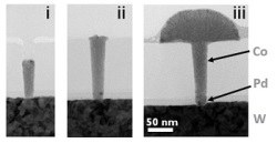
Imec, Belgium, and Lam Research Corp., Fremont, Calif., have reportedly developed a novel bottom-up prefill technique for vias and contacts for electronic chips. The technique, based on electroless deposition (ELD) of cobalt, is a highly selective method resulting in void-free filling of via and contact holes. Potentially increasing circuit performance, it is a promising path to scaling advanced interconnects and enabling future logic and DRAM nodes at the 7 nm node and below.
Engineers have demonstrated a cobalt ELD technique as a feasible method for highly selective bottom-up contact fill and via prefill with cobalt as an alternative metal to copper. Moreover, the high selectivity of the ELD process, at lower cost than chemical vapor deposition, ensures an intrinsically good metal-to-metal interface and paves the way to void-free via filling and increased yield.
As logic and memory nodes scale, performance of these advanced interconnects is negatively impacted by increasing interconnect resistance. In addition, voids in heavily scaled vias severely impact yield.
Trench-fill yield and line resistance may also benefit from the de-coupling of line and via aspect ratios, permitting the design of each for optimum resistance/capacitance. Therefore, cobalt prefilled ELD has the potential to enable future scaling of advanced logic and memory technologies.
The results were achieved in cooperation with Imec’s key partners as part of its core CMOS programs: GlobalFoundries, Intel, Samsung, SK Hynix, Sony, TSMC, Amkor, Micron, Utac, Qualcomm, Altera, Fujitsu, Panasonic, and Xilinx.