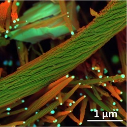
Thermo Scientific, Waltham, Mass., has developed the Verios G4 scanning electron microscope, which extends sub-nanometer resolution over the full 1 keV to 30 keV energy range to novel materials, such as catalyst particles, nanotubes, porosities, interfaces, and other nanoscale structures. High-resolution, high-contrast images are obtained without the need to transition to TEM or other imaging techniques.
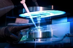
The instrument offers the flexibility required for research applications to accommodate large specimens such as full wafers or metallurgical samples. You can perform fast analysis thanks to its high current mode, or work on precise prototyping applications such as electron beam-induced direct deposition of materials or lithography.
The Verios G4 provides the excellent contrast needed for precise measurements on materials in a variety of applications without compromising the high throughput, analytical capabilities, sample flexibility, or operating ease of a traditional SEM. It features unique technologies such as constant power lenses for higher thermal stability and electrostatic scanning for higher deflection linearity. It is extremely flexible when it comes to choosing parameters, working on large samples, or supporting additional applications such as analysis or lithography. It allows both occasional users and specialists to access accurate and complete nanoscale data in the shortest time, discovering information that has been unavailable from other techniques.
https://www.fei.com/semicondutors/newst-innovative-products-2018/