Applied Materials Inc., Santa Clara, Calif., announces the opening of the Materials Engineering Technology Accelerator (META Center), a first-of-its-kind facility aimed at speeding customer prototyping of new materials, process technologies, and devices. As chipmaking becomes increasingly challenging, the META Center extends Applied’s ability to collaborate with customers to pioneer new ways of improving chip performance, power, and cost.
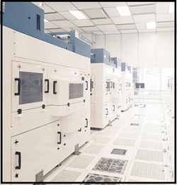
Located at the State University of New York Polytechnic Institute (SUNY Poly) campus in Albany, New York, the META Center’s cleanroom provides customers and partners access to state-of-the-art process systems to help shorten the time from lab to fab.
“Applied Materials welcomes innovators from established and emerging fields to work with us at the META Center to speed the commercialization of new technologies for the AI Era,” said Om Nalamasu, CTO of Applied Materials and president of Applied Ventures.
At the META Center, engineers can evaluate novel chip materials, structures and devices, testing them in a robust pilot manufacturing environment and accelerating their readiness for customer high-volume manufacturing facilities. Among the first chip devices under evaluation at the META Center is a new magnetic random-access memory (MRAM) targeted at Internet of Things devices, providing low-power, nonvolatile code storage and high-density working memory.
Applied’s recently launched Endura Clover MRAM PVD platform is among the systems at the META Center enabling this capability. The META Center is a strategic addition to Applied’s global R&D environment.