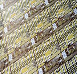
Researchers from Imec and KU Leuven University, Belgium, reported on and demonstrated a new methodology for the localization of dielectric breakdown sites in through-silicon via structures at the ASM International ISTFA 2019 conference in Portland, Ore. They applied an optical beam-induced resistance-change measurement and mechanical/chemical chip deprocessing to localize nm-sized pinhole breakdown sites in a high aspect-ratio 3×50 µm TSV array.
Thanks to the wavelength-selective absorption process in silicon, they could extract valuable defect depth-localization information from the laser stimulation measurement. After chip deprocessing, they inspected and localized the defect site in the dielectric liner by means of a scanning electron microscope. They confirmed results and analysis by cross-sectioning a TSV with a focused-ion beam.
Title: Localization of dielectric breakdown sites in 3D through-silicon via (TSV) interconnects by laser stimulation and chip deprocessing
Authors: Dr. Kristof J.P. Jacobs, Dr. Yunlong Li, Mr. Stefaan Van Huylenbroeck, Dr. Eric Beyne, Imec, Leuven, Belgium. www.imec-int.com
Prof. Ingrid De Wolf, KU Leuven, Leuven, Belgium