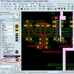
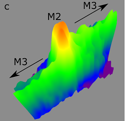
Engineers from Synopsis in Mumbai, India, and Mountain View, California, reported on a CAD-based technique utilizing IC design schematics for fast and accurate fault localization, at the ASM International ISTFA 2019 conference in Portland, Oregon. They also discussed some of the most effective methodologies for efficient root-cause analysis
In modern-day semiconductor failure analysis, the need for computer-aided design has extended beyond the sole physical layout to a much larger scope of integrated circuit design data, such as the source schematic and netlist. Due to the improved accuracy of predicted failures reported by test and diagnosis tools, it has become virtually mandatory to correlate the potential failing schematic features (e.g., nets and instances) to their corresponding location on the physical-CAD layout and actual device under test.
As technology nodes continue to shrink, systemic defects due to design-process interactions are a dominant component of integrated circuit yield loss. Shrinking nodes have continually increased the need for CAD-based FA techniques to isolate defects in ICs. Electrical fault isolation becomes more complex with added levels of interconnects, smaller feature sizes, and higher transistor densities in leading node ICs. These challenges significantly increase FA cycle time.
Fast and Accurate Fault Localization Through Effective Use of Design Schematics
Dr. Ankush Oberai, Synopsys Inc. Mountain View, California; [email protected]; Ph: +1-408-888-3542
Rupa Kamoji, Synopsys India Pvt. Ltd. Mumbai; [email protected] ; Ph: +91-22-61649598
Arpan Bhattacherjee; Synopsys Inc., Mountain View, California; [email protected] ; Ph: +1-510-468-9009