Engineers from NXP Semiconductors, Sector Technologies, and Thermo Fisher Scientific, reported that the application of IR-lock-in thermography has been extended from 2D and 3D package fault isolation to on-die level analysis, at the ASM International ISTFA 2019 conference in Portland, Oregon. In addition, the technique has become more sensitive, allowing for detection of much lower dissipated power.
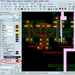
In this paper, several fault localization cases covering PCB assemblies down to die level analysis were discussed using IR-LIT and absolute temperature mapping. Where possible, the analysis was complemented with physical defect verification. The fault isolation cases include an ultra-low power dissipation (<150 nW) and several case studies with high ohmic connections.
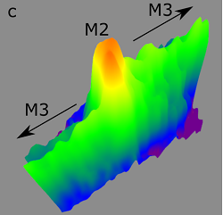
For the latter, a new method based on phase mapping was discussed, allowing for 2D localization of thermally invisible defects. The method was demonstrated on a test vehicle where phase data extracted from a visible feature of the device under test was studied. After this, a case study at die level was presented in an attempt to distinguish the phase information from two stacked M2-M3 metallization layers of the Back-End Of the Line (BEOL).
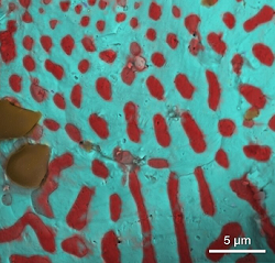
Finally, temperature mapping results of a five-micron-wide aluminum feature in silicon-oxide that was pushing the optical resolution of the tool was presented.
Infrared Lock-In Thermography: from localization of low power and masked defects to absolute temperature mapping for product debug
J. Jalink, A. Firiti, J. Van Den Biggelaar, NXP Semiconductors, The Netherlands;
A. Reverdy, Sector Technologies, France;
B. Lai, ThermoFisher Scientific, Fremont, California