Researchers at the University of New South Wales’ (UNSW) School of Chemical Engineering, Sydney, Australia, have developed a new approach to deposit large scale ultrathin semiconductors without grain boundaries using liquid metals.
Moore’s law, the empirical suggestion that the number of transistors doubles every few years in integrated circuits (ICs) has started to fail. Transistors are now so small that current silicon-based technologies are unable to offer further opportunities for shrinking. One possibility of overcoming Moore’s law is to resort to two-dimensional semiconductors.
Two-dimensional semiconductor materials are so thin that they allow free charge carriers (electrons and holes) to propagate in transistors along an ultrathin plane. Confining the charge carriers can potentially allow the semiconductor to switch very easily.
It can also provide directional pathways for the charge carriers to move without scattering, leading to transistors with infinitely small resistance. In theory, two-dimensional materials could result in transistors that do not waste energy switching on and off. Theoretically, they can switch very fast and ideally, switch off to absolute zero resistance values during their non-operational states.
One barrier preventing the construction of perfect ultrathin semiconductors with current technologies is that deposited ultrathin films are full of grain boundaries. Charge carriers bounce back from them increasing their resistive loss.
For the past two decades, molybdenum disulphide (MoS2) has been investigated as an ultrathin semiconductors for its electronic properties. Grain-boundary-free MoS2 is essential for making ICs, but it has yet been reached with acceptable maturity. It has proven to be a challenge to obtain very large-scale two-dimensional MoS2 without any grain boundaries using current large-scale deposition technologies. UNSW researchers created a new approach to grain-boundary-free deposition using liquid metals.
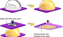
“This unique capability was achieved with the help of gallium metal in its liquid state. Gallium is an amazing metal with a low melting point of only 29.8 degrees C. It means that at a normal office temperature it is solid, while it turns into a liquid when placed at the palm of someone’s hand. It is a melted metal, so its surface is atomically smooth. It is also a conventional metal which means that its surface provides a large number of free electrons for facilitating chemical reactions,” said Yifang Wang, the first author of the paper.
“By bringing the sources of molybdenum and sulfur near the surface of gallium liquid metal, we were able to realize chemical reactions that form the molybdenum sulfur bonds to establish the desired MoS2. The formed two-dimensional material is templated onto an atomically smooth surface of gallium, so it is naturally nucleated and grain boundary free. This means that by a second step annealing, we were able to obtain very large area MoS2 with no grain boundary. This is a very important step for scaling up this fascinating ultra-smooth semiconductor.”
The UNSW researchers plan to expand their methods to create other two-dimensional semiconductors and dielectric materials that can be used as different parts of transistors.
For more information:
University of New South Wales
http://www.unsw.edu.au/