For the first time, a team of scientists from SLAC National Accelerator Laboratory, Stanford University, Pennsylvania State University, Purdue University, and Hewlett Packard Labs have used ultrafast electron diffraction (UED), an ultrafast camera to observe for the first time the atomic and electronic movements as miniature vanadium dioxide-based switches operated.
The electronic device in the research, published in Science, is a custom-designed miniature switch made of vanadium dioxide. This material can switch between electrically insulating and conducting states. The researchers toggled the switches electrically while taking snapshots that showed subtle changes in the atomic arrangement over millionths of a second. These changes correlated with the time-dependent flow of electrons through the switch, enabling the discovery of a short-lived intermediate state. This finding could lead to faster and more energy-efficient computing devices.
The team discovered a short-lived state that could lead to faster and more energy-efficient switching. The research also provides invaluable data on microscopic phenomena that occur during device operations, which is crucial for designing circuit models in the future.
This research reports on the operation of electronic switches based on vanadium dioxide, a quantum material. The results identify the ultimate limits to the device’s switching speed and show that the switch operates over millions of cycles. These insights may lead to engineering the material to make the newly discovered state more stable and longer lasting. These advances could enable devices in which switching occurs with minimal atomic motion, enabling faster operation and requiring lesser energy. This approach may also lead to new ways of using pulsed electric fields to create novel materials with useful properties.
This research offers a new way of designing materials that do not exist under natural conditions, allowing scientists to observe them on ultrafast timescales and then potentially tune their properties. This approach will enable the creation of next-generation electronic devices that can meet the world’s growing needs for data-intensive, intelligent computing.
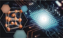
Image – A new method captured the ultrafast atomic motions inside the tiny switches that control the flow of current in electronic circuits based on vanadium dioxide, whose crystal structure is shown on the left. Courtesy of: SLAC National Accelerator Laboratory.
For more information:
Hewlett Packard Labs
https://www.hp.com/us-en/hp-labs.html
Pennsylvania State University
Purdue University
SLAC National Accelerator Laboratory
https://www6.slac.stanford.edu/
Stanford University