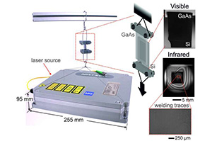
Laser micro-welding is an advanced manufacturing method today applied in various domains. However, important physical limitations have prevented its applicability in silicon and other technology-essential semiconductors. Concentrating on circumventing the optical limits on the deliverable energy density at interfaces between narrow-gap materials with intense infrared light, the first feasibility demonstration of transmission laser welding between Si workpieces using nanosecond laser pulses is made. A shear joining strength of 32 ± 10 MPa which compares very favorably to the complex process alternatives is obtained.
This successful experiment, now published in Laser & Photonics Reviews, confirms a technological barrier that has been definitively lifted. Compared to alternative methods in the semiconductor industry, a unique advantage of laser micro-welding is the ability to join elements with complex multi-material architectures in a direct-write manner that would not be possible otherwise. This should lead to new modalities for manufacturing in electronics, mid-infrared photonics, and microelectromechanical systems (MEMS). Moreover, we envision the potential for the emerging concepts of hybrid chips, including electronics and microfluidics functions for the thermal management of the most demanding micro-technologies, such as super-computers or advanced sensors.
For more information: Science X Dialog