Intel Corp., Santa Clara, Calif., unveiled research breakthroughs fueling its innovation pipeline for keeping Moore’s Law on track to a trillion transistors on a package in the next decade. Intel researchers made advancements in 3D packaging technology with a new 10x improvement in density, novel materials for 2D transistor scaling beyond RibbonFET, including super-thin material just 3 atoms thick, new possibilities in energy efficiency and memory for higher-performing computing, and advancements for quantum computing.
Moore’s Law is vital to addressing the world’s insatiable computing needs as surging data consumption and the drive toward increased artificial intelligence (AI) brings about the greatest acceleration in demand ever.
Continuous innovation is the cornerstone of Moore’s Law. Many of the key innovation milestones for continued power, performance and cost improvements over the past two decades – including strained silicon, Hi-K metal gate and FinFET – in personal computers, graphics processors and data centers started with Intel’s Components Research Group. Further research, including RibbonFET gate-all-around (GAA) transistors, PowerVia back side power delivery technology and packaging breakthroughs like EMIB and Foveros Direct, are on the roadmap today.
Intel’s Components Research Group has committed to innovating across three key areas to continue Moore’s Law: new 3D hybrid bonding packaging technology to enable seamless integration of chiplets; super-thin, 2D materials to fit more transistors onto a single chip; and new possibilities in energy efficiency and memory for higher-performing computing.
The Components Research Group researchers have identified new materials and processes that blur the line between packaging and silicon. We reveal critical next steps on the journey to extending Moore’s Law to a trillion transistors on a package, including advanced packaging that can achieve an additional 10x interconnect density, leading to quasi-monolithic chips. Intel’s materials innovations have also identified practical design choices that can meet the requirements of transistor scaling using novel material just 3 atoms thick, enabling the company to continue scaling beyond RibbonFET.
Intel also introduced quasi-monolithic chips for next generation 3D packaging. Intel’s latest hybrid bonding research shows an additional 10 times improvement in density for power and performance over Intel’s IEDM 2021 research presentation. Continued hybrid bonding scaling to a 3 um pitch achieves similar interconnect densities and bandwidths as those found on monolithic system-on-chip connections.
Looking to super-thin ‘2D’ materials to fit more transistors onto a single chip, Intel demonstrated a gate-all-around stacked nanosheet structure using 2D channel material just 3 atoms thick, while achieving near-ideal switching of transistors on a double-gate structure at room temperature with low leakage current. These are two key breakthroughs needed for stacking GAA transistors and moving beyond the fundamental limits of silicon. Researchers also revealed the first comprehensive analysis of electrical contact topologies to 2D materials that could further pave the way for high-performing and scalable transistor channels.
To use chip area more effectively, Intel redefines scaling by developing memory that can be placed vertically above transistors. In an industry first, Intel demonstrates stacked ferroelectric capacitors that match the performance of conventional ferroelectric trench capacitors and can be used to build FeRAM on a logic die.
An industry-first device-level model captures mixed phases and defects for improved ferroelectric hafnia devices, marking significant progress for Intel in supporting industry tools to develop novel memories and ferroelectric transistors.
Bringing the world one step closer to transitioning beyond 5G and solving the challenges of power efficiency, Intel is building a viable path to 300 millimeter GaN-on-silicon wafers. Intel breakthroughs in this area demonstrate a 20 times gain over industry standard GaN and sets an industry record figure-of-merit for high performance power delivery.
Intel is making breakthroughs on super-energy-efficient technologies, specifically transistors that don’t forget, retaining data even when the power is off. Already, Intel researchers have broken two of three barriers keeping the technology from being fully viable and operational at room temperature.
Intel continues to introduce new concepts in physics with breakthroughs in delivering better qubits for quantum computing. Intel researchers work to find better ways to store quantum information by gathering a better understanding of various interface defects that could act as environmental disturbances affecting quantum data.
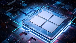
Image – Intel targets new 10x density improvement in packaging technology and uses novel material just 3 atoms thick to advance transistor scaling.
For more information:
Intel Corporation