Imec, Belgium, and Coventor, Cary, N.C., announce the expansion of a joint development project to explore process variation issues in 7 nm semiconductor technology. For over a year, the joint team has been using Coventor’s semiconductor process modeling platform, SEMulator3D, to perform predictive modeling of semiconductor fabrication processes and to proactively analyze process variation issues in 7nm semiconductor technology. The collaboration has now been expanded beyond logic-only devices to include 3D NAND Flash, STT-MRAM, and other device types.
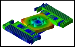
A highlight of the collaboration has been a massive process simulation experiment to explore the effect of process variability in 7nm BEOL (back end of line) fabrication processes. Researchers used SEMulator3D to simulate an entire window of process variability, which would have required more than one million actual semiconductor wafers if conventional testing methods had been used. This experiment was made possible by the robust virtual fabrication environment of SEMulator3D using a fully codified 7nm process flow, along with the ability to support parallel distributed computing and a novel algorithm for submitting variation cases to the simulator. With these powerful tools, the team was able to produce key findings that will help advance 7nm semiconductor technology.
“We have worked with Imec to accelerate the state of the art in semiconductor process technology useful in a broad range of next-generation devices such as Logic, 3D NAND Flash, STT-MRAM, and others,” said David Fried, Chief Technical Officer at Coventor. “By providing our customers with a comprehensive virtual fabrication environment, plus our combined expertise, Coventor and Imec are reducing the time and cost associated with moving to these emerging semiconductor nodes.”