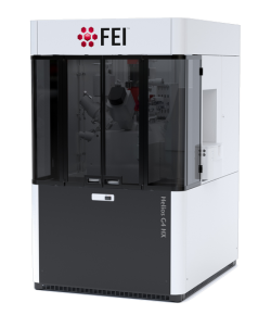
FEI Co., Hillsboro, Oregon, announces that the new Helios G4 HX utilizes a patented inverted TEM sample preparation method to create high-quality lamellas for the most advanced semiconductor nodes. Integrating FEI’s EasyLift EX Nanomanipulator, new Automated QuickFlip shuttle, and iFast automation software platform, the Helios G4 HX provides value to failure analysis labs by means of a fully integrated, automated solution.
Improved materials contrast enabled by low-loss in-lens detectors, along with extreme high-resolution SEM imaging at low-kV, ensures accurate endpointing, which results in increased yield during final thinning of the TEM sample.
The instrument combines the industry-leading, highest-resolution, highest-contrast Elstar+UC SEM with the most advanced Phoenix FIB for best-in-class imaging and milling performance. Specifically designed for high-throughput, high-quality, ultra-thin TEM lamella preparation, the Helios G4 HX comes with the FEI EasyLift EX Nanomanipulator and new Automated QuickFlip shuttle for precise, accurate, and repeatable in situ sample lift-out and manipulations. When used in conjunction with the FEI iFast Starter Recipes for automated TEM sample preparation, even novice operators are able to repeatedly create high-quality, ultra-thin lamellas with confidence.
The Helios G4 HX is designed to meet the challenges of advanced semiconductor failure analysis labs. The FEI Cell Navigator accurately locates the defect in repeating structures using automated sample navigation. This improves the success rate of finding the intended region of interest by greater than 5%. In addition, the patented inverted TEM sample preparation method, enabled by the FEI EasyLift EX Nanomanipulator, new Automated QuickFlip shuttle, and automation software platform iFAST, delivers the highest throughput in the industry.