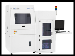
Rudolph Technologies, Flanders, N.J., introduces the NSX 330 Series, which combines defect inspection with 2D and 3D metrology. It enables advanced packaging processes with a combination of inspection plus metrology approach. NSX 330 Series includes 100% wafer level metrology for micro bumps, RDL, kerf, overlay, and through silicon via (TSV) in a single wafer load.
The NSX 330 Series builds on the advancements in platform technology offered by the NSX 320 System: high-acceleration staging, high-speed multi-processor computing, and highly flexible software with an unprecedented level of usability. To this field-proven product, the NSX 330 Series adds increased 2D inspection and metrology throughput, and a broad portfolio of 3D sensors supporting the following critical applications:
- 100% bump height metrology
- Simultaneous high accuracy topography, depth and thickness measurements
- Substrate thickness, TTV, and bonded wafer thickness stack thickness (carrier, adhesive, product wafer and total stack)
- Via depth (unlimited aspect ratio)
- Thick and thin RST
- Bow and warp.
The system is designed for advanced packaging with combination inspection and metrology, 40% faster inspection scans, simultaneous topography and thickness measurements down to nanometer resolution, laser triangulation-based 100% bump height and coplanarity at 0.1µm, and much more.