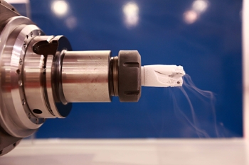
3D-Micromac AG, Chemnitz, Germany, introduces the Microprep 2.0 laser ablation system for high-volume sample preparation of metals, semiconductors, ceramics and compound materials for microstructure diagnostics and failure analysis. As the first stand-alone, ultrashort pulsed laser-based tool for sample preparation, the system enables large-area and 3D-shape sampling for more comprehensive testing of complex structures.
Built on a highly flexible platform with a small table-top footprint, the system is easily integrated into failure analysis workflows, and samples can be moved between FA tools using the same pin stubs and holders, providing ease of use and time savings.
Developed jointly with Fraunhofer Institute for Microstructure of Materials and Systems, Munich, Microprep complements existing approaches to sample preparation such as focused ion beam (FIB) micromachining, offering up to 10,000 times higher ablation rates and therefore an order of magnitude lower cost of ownership compared to FIB.
The system significantly accelerates critical steps used in FIB micromachining, which can take several hours for very small sample sizes. By off-loading the vast majority of sample prep work from the FIB tool and relegating FIB to final polishing or replacing it, completely depending on application, time to final sample can be reduced to less than one hour in many cases.
Applications range from in-plane geometries and bulk samples to cross-sections, box milling (such as for diagnostics of electrical connections and 3D chip-level structures),and full line cut (for complex investigations of complete devices).