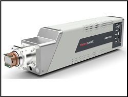
Thermo Scientific, Waltham, Mass., introduces the Lumis EBSD detector, which can rapidly identify crystallographic phases, grain sizes, and orientation, as well as monitor structural transformations in SEM samples. The instrument is designed for maximum throughput and high resolution, and incorporates new CMOS sensor technology and advanced optics, which is harnessed with Thermo Scientific Pathfinder 2.0 microanalysis software that includes new indexing algorithms for the analysis of electron backscatter patterns (EBSPs).
The Lumis EBSD detector incorporates the most developed CMOS sensor technology available with advanced optics and accelerating indexing algorithms for the analysis of electron backscatter patterns using probe currents down to 10 pA and below. With pattern collection at >2.2 million pixels, the detector is ideally suited to HR-EBSD strain measurement and phase identification applications.
Using optical and sensor binning, the detector can be optimized for high speed EBSD at several thousand frames per second for reduced collection times and higher sample throughputs. The advanced optics and high sensor sensitivity allow EBSPs to be acquired at ultra-low probe currents below 10 pA. This is particularly important for beam sensitive and dose-restricted materials, or in cases where higher probe current may introduce contamination or drift.
A large-format CMOS sensor and a patented reverse zoom optic complement and extend the built-in CMOS sensor binning. A high efficiency, octagonal scintillator converts the electron backscatter electrons into light, which is focused onto a user-controlled region of the sensor by the high-quality reverse zoom optic. This allows a continuous choice of “binned” EBSP size and gives full flexibility over EBSP speed, quality, and sensitivity.