Engineers from Nikon Metrology Inc. discussed x-ray technologies and techniques that can provide visualization and metrology analysis of semiconductor chips, at the ASM International ISTFA 2019 conference in Portland, Oregon. In this paper, the authors discuss modern 2D and 3D x-ray based approaches for testing and failure analysis, and describe how these different methods have practical application for failure analysis and dimensional metrology.
With new developments in software, 2D and 3D x-ray techniques for testing and failure analysis allow for the extraction of internal features in a nondestructive fashion with resolutions in the range of 1 µm or less. Current 3D x-ray technologies have the ability to generate geometric data for a complete characterization of material structures (including external features) and detect manufacturing defects and dimensional deviations from intended design.
To study complex structures produced by a manufacturing process with current NDT technologies, CT might be the only available technology that can accurately—i.e., with small uncertainty (< 10µm)—determine dimensions of inner or hidden structures in an assembled product.
With a destructive method, the dimensions extracted from the disassembled state of a product may differ from the actual geometrical dimensions in the original assembled state. This is particularly relevant for parts built with a variety of manufacturing processes, including additive manufacturing.
In addition, x-ray technologies can be used as a quality control tool from optimization to production, or to quickly identify or even prevent failures (inspection time can vary from a few seconds to tens of minutes), which saves both money and time.
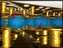
Image shows a CT scan of an electronics chip in which the different BGA layers and bond wires are segmented by color. (Cracks and voids in the balls are shown).
Title: Modern 2D & 3D x-ray technologies for testing and failure analysis
Herminso Villaraga-Gómez and Joshua D. Bell, Nikon Metrology Inc., Brighton, Michigan