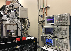
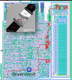
Engineers from Thermo Fisher Scientific presented a discussion of a technique in which the voltage-contrast mechanism of a scanning electron microscope is used to probe electrical waveforms on FinFET transistors that are located within active integrated circuits.
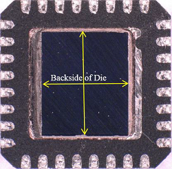
The FinFET devices are accessed from the backside of the integrated circuit, enabling electrical activity on any transistor within a working device to be probed. We demonstrate gigahertz-bandwidth probing at 10-nm resolution using a stroboscopic pulsed electron source.
There is an unmet need for performing failure analysis (FA) with high spatial and temporal resolution on integrated circuits (ICs) having 10-nm or smaller feature sizes. The current generation of FA tools employs optical techniques to localize defects in the design or manufacture of ICs, yet minimum IC feature sizes have become too small to be resolved optically. As a result, a transition from optical imaging to imaging using a scanning electron microscope (SEM) appears warranted.
This paper addresses whether a SEM-based FA tool can – in addition to achieving high spatial resolution – also enable high-bandwidth waveform measurements from active modern IC devices. A challenge along this path is that the temporal bandwidth of secondary-electron detectors (SEDs) used with SEMs is typically limited to 10 MHz, which necessitates a non-standard solution to meet the high-temporal resolution demanded by the FA community.
Failure Analysis of FinFET Circuitry at GHz Speeds using Voltage-Contrast and Stroboscopic Techniques on a Scanning Electron Microscope
James Vickers, Seema Somani, Blake Freeman, Thermo Fisher Scientific, Fremont, California
Pete Carleson, Thermo Fisher Scientific, Hillsboro, Oregon
Lubomír Tůma, Marek Unčovský, Petr Hlavenka,, Thermo Fisher Scientific, Brno, Czech Republic