As global electricity demand and supply grow, efficient power electronics are crucial for enhancing grid efficiency, stability, integration, and resilience across all energy sources. Advances in wide-bandgap semiconductor materials promise greater power handling capabilities while reducing electrical and thermal losses, enabling the development of smaller, faster, more reliable, and energy-efficient power electronic components compared to current silicon-based technologies.
Researchers from the National Renewable Energy Laboratory (NREL), the Colorado School of Mines, and Oak Ridge National Laboratory examined a potential route to achieve peak performance of aluminum gallium nitride, AlxGa1–xN, a key material for increasing power electronics’ energy efficiency and performance, through growth on optimized substrate materials.
This work was undertaken with funding support from the microelectronics initiative through the U.S. Department of Energy Basic Energy Sciences Office and Advanced Scientific Computing Research program.
The goal of the work is to grow higher-quality materials through the selection of a lattice-matched substrate. Better electron transmission means better device performance, but the growth of AlxGa1–xN on lattice-mismatched substrates leads to dislocation (line defects that distort a lattice due to the misalignment of atoms), resulting in diminished performance.
“Substrate engineering enables the use of high-performing materials in real devices,” said NREL’s Dennice Roberts, a materials science researcher. “If we can engineer lattice-matched substrates to reduce the effect of dislocations, we can widen the range of sufficiently high-quality materials and build better, more energy-efficient power electronics.”
Substrate engineering can improve device performance—but it is complicated. Defects, such as substrate cracking, are common with growth on AlN and GaN. Efforts to reduce dislocation have been effective but often increase device complexity and limit device design and performance. Lattice mismatching, again, leads to device performance issues.
“Lattice matching is critical for high-quality epitaxial growth,” Roberts said. “We hypothesized that substrates from transition metal carbide and nitride families could enable desired conditions for AlxGa1–xN growth, not only because of ideal lattice matching but also because of ideal thermal and electrical conductivity properties. TaC and AlxGa1–xN are closely lattice-matched, TaC is highly conductive, and they display matched growth in size in response to changes in temperature.”
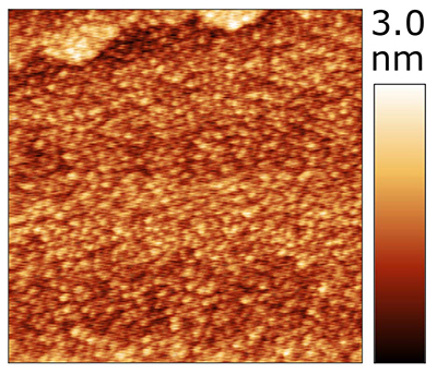
The team grew, prepared, and used TaC thin films as virtual substrates for high-aluminum-content AlxGa1–xN and demonstrated AlxGa1–xN growth on TaC virtual substrates. To precisely and effectively deposit TaC onto the substrate, they used radio frequency sputtering. They formed substrates through high-temperature annealing, a process that increases ductility—the ability of a metal to undergo significant stress before cracking or breaking—and reduces defects.
For more information: PRX Energy