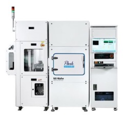
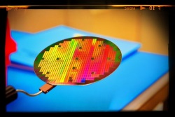
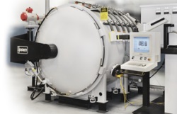
Park Systems, Santa Clara, Calif., announces Park NX-Wafer, an AFM designed for bare wafer manufacturing that fully automates the automatic defect review process. Park says that new AFM increases production throughput by 1000%. Park NX-Wafer produces sub-Angstrom roughness measurements for the flattest substrates and wafers with tip-to-tip variation of less than 2%, for the first time ever. This fully automated defect review and identification system enables a critical inline process to classify defect types and source their origin through high-resolution 3D imaging.
“Park NX-Wafer is an updated continuation from the wafer metrology product line, the Wafer Series, with new application capabilities focusing on automatic defect review (ADR), atomic force profiler, and sub-Angstrom surface roughness control. Among the three, SmartADR for 200/300mm bare wafers is a disruptive technology that improves productivity by up to 1000% compared to traditional defect review methods by AFM,” explains Sang-il Park, CEO and Chairman Park Systems
“Designed specifically for the semiconductor industry, the new bare wafer ADR is the most advanced, fully automated defect review solution available, featuring advanced coordinate translation with enhanced vision that does not require any separate steps to calibrate the stage of the targeted defect inspection system, or labor-intensive reference marking on the target wafer sample. The AFM-based defect review enables non-destructive 3D imaging of defects as small as a few nanometers.”
NX-Wafer has several new features , including a long-range sliding stage that combines with NX-Wafer to become an Atomic Force Profiler (AFP). The new low noise AFP provides very flat profiling up to 50mm with profiling speed as fast as 1mm/sec for both local and global uniformity measurements. Another new feature is the fully automated defect review process from transfer and alignment of defect maps to the survey and zoom-in scan imaging of defects on 200/300mm bare wafers. By utilizing Park’s proprietary coordinate translation technique via enhanced vision, the new bare wafer ADR can accurately transfer the defect maps obtained from a laser-scattering defect inspection tool to the Park NX-Wafer system.