The University of Oregon, Eugene, announces that its researchers have created STEM holography, a new technique that provides improved atomic resolution of a material’s outer structure and unveils previously unseen interfaces between the surface and the underlying material.
In STEM holography, electrons are sent along two separate paths, one going through the sample and one not. The time delay between electrons in reaching the target is measured, and this enables researchers to build a high-resolution image.
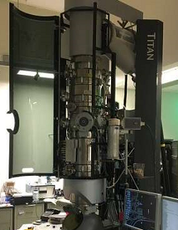
The multimillion-dollar microscopes create micrographs as a beam of electrons passes through a thin slice of a material. Traditionally in scanning transmission electron microscopes, magnetic fields are used to focus the beam to an atom-sized spot. That beam then is scanned across the sample, but large numbers of electrons are required to see anything because most of them go through without being deflected.
UO researchers, using microscopes at the university, Lawrence Berkeley National Laboratory, and Hitachi Ltd.’s R&D Group in Japan — have now shown that STEM holography works.
“We put the electron microscope in conditions where we could isolate the signal that we care about, and we looked at several different kinds of materials,” said former UO doctoral student Tyler Harvey, now a postdoctoral researcher at the University of Gottingen. “We also simulated images of one sample and found that the simulations matched the experiment very well.” In a December paper led by Dr. Harvey in the journal Physical Review Applied, the UO team described the technique and discussed how it works theoretically.
The Oregon researchers placed a diffraction grating above the sample, creating additional beams hitting the sample and a hologram below it. That captures signals from electrons that are not scattered, and details about how others are slowed as they pass through a sample. The researchers have tested their technique on gold nanoparticles, carbon substrates, and electrical fields.
“This technique allows us to study a material’s structure at high resolution, measure structures accurately, and understand them better than was possible before,” said doctoral student Fehmi Yasin. “Previously, the field of view of STEM holography was limited to maybe 30 nanometers. Flexible STEM holography expands the field of view.”
https://around.uoregon.edu/news