Researchers from ON Semiconductor, Phoenix, addressed the challenges for FA engineers in fault localization when analyzing a die, at the ASM International ISTFA 2019 conference in Portland, Oregon.
This paper discusses integrating EOP techniques in traditional FA to localize failure in mixed signal ICs. The three case studies presented establish the technique to be effective, quick, and easy to probe non-invasively with minimal backside sample preparation.
Techniques such as electro optical probing (EOP) or laser voltage probing (LVP) can acquire electrical signals on transistors and create an activity map of the circuitry. In failure analysis, they are applied to localize defects.
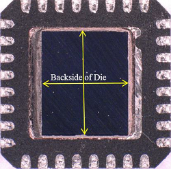
The most significant benefit of EOP is the accessibility of the nodes with minimal sample preparation. For example, there is no need of a probe pad and simple backside thinning is sufficient. This makes EOP a much faster, non-destructive, contactless analysis technique. EOP is a very versatile technique that has proven to be useful on many different devices.
In this paper, we evaluated better ways to analyze clock skew delay, abnormal transistor switching, and clock shoot-through by applying EOP for acquiring timing and fault information. The case studies demonstrate the EOP technique to be an effective, nondestructive localization technique combined with traditional PEM and OBIRCH. They show that EOP could be easily implemented to check the activity of the transistors in the suspect area with simple backside thinning and not requiring creation of FIB probe pads.
With this technique, the turnout time for fault localization of a component/failing block could be significantly reduced. Furthermore, EOP analysis can be improved with a redesigned Evaluation Board with wider opening; or with a backside repackaging method for using the SIL.
Case Studies on Application of Electro Optical Probing (EOP) – A Noninvasive Backside Localization Technique in Failure Analysis
Srinath Rajaram, Rajesh Kabadi, and Eric Barbian, Product Analysis Lab, ON Semiconductor, Phoenix, Arizona