Agile Analog, an analog IP company based in the U.K., recently completed a set of key analog IP to assist with IoT design: basic analog building blocks to enable faster IoT design without requiring a custom in-house design. Despite the prominence of digital technologies in the IoT world, analog circuits are still a major requirement for high-performance chip design. With Agile’s Foundation IP, designers may implement analog building blocks within their designs to match their requirements and ensure optimal performance.
The global impact of digital electronics is immeasurable. From solving differential equations to securely encoding messages, digital electronics are largely responsible for everyday computing as we know it. Despite this, analog electronics are integral to many systems.
Even the simplest digital chips require some power conditioning to ensure proper voltages are applied to the power rails. As digital circuits become more complex, more analog functions are required, such as low-noise amplifiers (LNAs), data converters, oscillators, and many more.
Agile Analog’s goals are simple: provide designers with improved analog circuits while making integration for ASICs or SoCs easier. Using Agile’s Composa technology, designers are no longer limited to the IP available for their process of choice. Instead, the Composa methodology takes the chosen PDK as an input to develop the required analog deliverables, making the IP a multi-process solution.
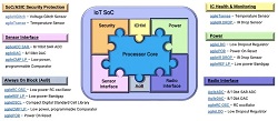
Knowing that analog design is not a large focus of an IoT designer, Agile Analog has set out to make the analog design process as easy as possible with its Foundation IP. The Foundation IP consists of six blocks:
- SoC/ASIC Protection
- Sensor Interface
- Always On Block
- IC Health Monitoring
- Power
- Radio Interface
Using the blocks, designers can abstract the analog design process and simply work with building blocks to accomplish the desired analog function.
After settling on a process node, Agile Analog’s Foundation IP may be used to generate high-performance analog circuits without an in-house hands-on design process. This allows IoT designers to focus on their own innovations and use Agile’s IP to fill in the blanks for analog design. It also helps to meet tapeout deadlines, improve time to market, and yield final chips that work as designed—helping to save on overall costs.
Agile’s Foundation IP is not a sign that the field of analog electronics is stagnating but rather a response to a relatively complicated design process when compared to digital electronics. Analog electronics are still undergoing innovation, but not all designers need these innovations.
Image – Agile Analog’s Foundation IP with each block’s components explained in further detail. Courtesy of: Agile Analog.
For more information:
Agile Analog