In a new study, researchers from Yale University (New Haven, Conn.) show that a mold about half the size of a fingernail could lead to the development of stronger, higher-performing materials for airplanes and other uses. Their novel method provides unique insight into the microstructure and properties of a metal and eliminates the limitations of more traditional analysis.
Jan Schroers, the Robert Higgin Professor of Materials Science & Mechanical Engineering, who led the study said that the chemistry and orientation of the grains control the material’s actual properties. But because the pattern of grains is not uniform throughout a piece of metal, different properties can show up in different places in the same piece of metal. That makes it difficult to tailor a piece of metal to a specific use.
If scientists had a clearer understanding and better control of the atomic structures of various metals, they could better understand, predict, and optimize materials for different purposes.
Up until now, there has been a trade-off between the two most common methods of analyzing a metal’s overall structure and properties, and neither produces a fully satisfying result.
Transmission electron microscopy (TEM) is one of the most prominent means of studying these structures. With TEM, an electron beam is shot into a piece of metal, getting a very clear snapshot of a very small area of that piece of metal. However, grain structures change throughout the same piece of metal, so that snapshot does not provide anything close to the full picture.
Conversely, researchers can apply a mechanical test to an entire piece of metal to determine its strength and other properties. “But in that case, you don’t really know what is going on microscopically,” Schroers said.
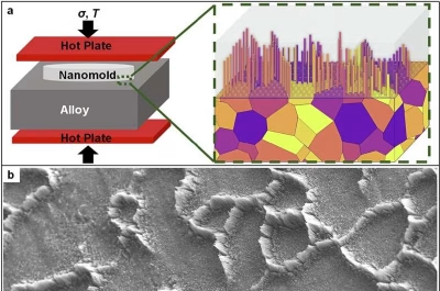
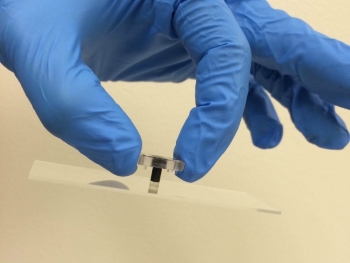
The solution comes in the form of a small, square mold with billions of nanosized holes. The process involves heating a piece of metal about the size of the mold and then pressing it against the mold. The metal passes through the holes, forming nanorods.
What caught the researchers’ attention when they first did this was that the nanorods varied dramatically in length, even though they applied the same pressure and temperature throughout the piece of metal.
Knowing where the nanorods were longer and shorter, they could see at a resolution of about 2.5 nanometers what the metal’s properties were over a large area and connect properties with its atomic structure at each location.
“So our technique closes this gap,” Schroers said. “We can measure over macroscopic dimensions that you can see with your naked eye, but we have very high microscopic resolution. This imprint gives us the characteristics of the material. It gives us a new tool, like a microscope.”
Image – Introduction of local deformation mapping (LDM). Courtesy of Nature Communications, 2026, doi.org/10.1038/s41467-026-75351-8.
************
For more information:
Yale University