Graphene is extremely strong and good at conducting heat and electrical currents, making it an exceptionally versatile material. Yet, many properties of the material are still poorly understood – for the simple reason that the atoms they are made up of are very difficult to observe. A team of researchers from the University of Amsterdam (UvA) and New York University have now found a surprising way to solve this issue.
Continue readingMysteries of atomically thin mica resolved
Mica, a common mineral found in granite, and has been extensively studied from geological, chemical, and technical perspectives. But recently a team from the Vienna University of Technology presented a study that explains the distribution of potassium ions on the mica surface. The researchers used a new type of atomic force microscope to conduct their investigation. Prior to this, the physical surface details of mica have never been studied on an atomic scale.
Continue readingNeutrons aid in discovery of strengthening behavior in alloys
Oak Ridge National Laboratory (ORNL) researchers used neutron diffraction to identify a mechanism in a 3D-printed alloy—coined “load shuffling”—that could enable the design of better-performing lightweight materials for vehicles.
Continue readingFormFactor opens Silicon Valley Demo Center
FormFactor, Inc., Livermore, Calif., a leading semiconductor test and measurement supplier, opened a new product demonstration and training center in San Jose, California. The facility is staffed with applications engineers and training professionals, and features
FormFactor engineering wafer probers, metrology systems and advanced probe cards outfitted to meet semiconductor test and measurement requirements from lab to fab, including solutions for advanced packaging, automotive high-power devices, high-speed digital, silicon photonics, and 5G/6G/millimeter-wave mobile devices.
“The opening of our new demonstration center provides easy access for our customers to see first-hand the benefits of our sophisticated wafer probe and metrology solutions,” said Amy Leong, senior vice president and chief commercial officer. “We are deeply committed to enabling industry innovation, and proud to offer this center to accelerate our customers’ success with personalized, hands-on training, product demonstration, and support.”
FormFactor’s new demonstration center is located in the heart of Silicon Valley and offers a product demonstration lab and clean room, presentation and training areas, service warehouse, office space and conference rooms. The new location complements the capabilities of FormFactor’s existing global demonstration centers in Europe and Asia, and recently opened Advanced Quantum Cryogenic Lab in Boulder, Colorado.
For more information:
FormFactor, Inc.
Perovskites, a ‘dirt cheap’ alternative to silicon, just got a lot more efficient
A study at the University of Rochester, Rochester, N.Y., suggests perovskites — a family of materials nicknamed for their crystalline structure that have shown extraordinary promise in recent years as a far less expensive, equally efficient replacement for silicon in solar cells and detectors — may become far more efficient.

Researchers typically synthesize perovskites in a wet lab, and then apply the material as a film on a glass substrate and explore various applications. Chunlei Guo, professor of optics at the University of Rochester leading the study reported in Nature Photonics, instead proposes a novel, physics-based approach.
By using a substrate of either a layer of metal or alternating layers of metal and dielectric material—rather than glass—he and his coauthors found they could increase the perovskite’s light conversion efficiency by 250 percent.
“No one else has come to this observation in perovskites,” Guo says. “All of a sudden, we can put a metal platform under a perovskite, utterly changing the interaction of the electrons within the perovskite. Thus, we use a physical method to engineer that interaction.”
Metals are probably the simplest materials in nature, but they can be made to acquire complex functions. The Guo Lab has extensive experience in this direction. The lab has pioneered a range of technologies transforming simple metals to pitch black, superhydrophilic (water-attracting), or superhydrophobic (water-repellent). The enhanced metals have been used for solar energy absorption and water purification in their recent studies.
In this new paper, instead of presenting a way to enhance the metal itself, the Guo Lab demonstrates how to use the metal to enhance the efficiency of pervoskites.
“A piece of metal can do just as much work as complex chemical engineering in a wet lab,” says Guo, adding that the new research may be particularly useful for future solar energy harvesting.”
In a solar cell, photons from sunlight need to interact with and excite electrons, causing the electrons to leave their atomic cores and generating an electrical current, Guo explains. Ideally, the solar cell would use materials that are weak to pull the excited electrons back to the atomic cores and stop the electrical current.
Guo’s lab demonstrated that such recombination could be substantially prevented by combining a perovskite material with either a layer of metal or a metamaterial substrate consisting of alternating layers of silver, a noble metal, and aluminum oxide, a dielectric.
The result was a significant reduction of electron recombination through “a lot of surprising physics,” Guo says. In effect, the metal layer serves as a mirror, which creates reversed images of electron-hole pairs, weakening the ability of the electrons to recombine with the holes.
The lab was able to use a simple detector to observe the resulting 250 percent increase in efficiency of light conversion.
Several challenges must be resolved before perovskites become practical for applications, especially their tendency to degrade relatively quickly. Currently, researchers are racing to find new, more stable perovskite materials.
“As new perovskites emerge, we can then use our physics-based method to further enhance their performance,” Guo says.
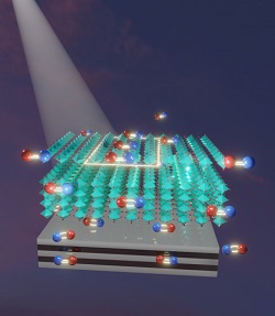
Image – This illustration from the Guo Lab shows the interaction between a perovskite material (cyan) and a substrate of metal-dielectric material. The red and blue pairings are electron-hole pairs. Mirror images reflected from the substrate reduce the ability of excited electrons in the perovskite to recombine with their atomic cores, increasing the efficiency of the perovskite to harvest solar light. Courtesy of: Chloe Zhang.
For more information:
University of Rochester
AI-designed chips reach scale with first 100 commercial tape-outs using Synopsys technology
Stacking LEDs instead of placing them side by side could enable fully immersive virtual reality displays
Electronic bridge allows rapid energy sharing between semiconductors
How to grow a tiny metallic snowflake
Scientists at the University of Auckland, New Zealand, are working at the level of atoms to create something unexpected: tiny metallic snowflakes. During their research, they discovered that interactions between the atomistic structures of various metals and liquid gallium cause differently shaped crystals to emerge.
Continue readingMicroscopy and modeling help examine battery wear and tear
Researchers at the University of Chicago’s Pritzker School of Molecular Engineering (PME) have now used a combination of high-powered electron microscopy and computational modeling to understand exactly what occurs, on an atomic level, when lithium-ion batteries degrade. Their research points toward one approach to designing longer-lasting lithium-ion batteries—by focusing on the carbon binder domain (CBD).
Continue readingThe answer to why Roman concrete is so durable
Researchers have spent decades trying to figure out the secret of Rome’s ultradurable ancient construction material, used in the famed Pantheon as well as aqueducts and seawalls that endured especially harsh environmental conditions. Now, a team of investigators from MIT, Harvard University, and laboratories in Italy and Switzerland, has made progress in this field, discovering ancient concrete-manufacturing strategies that incorporated several key self-healing functionalities.
For many years, researchers have assumed that the key to the ancient concrete’s durability was based on one ingredient: pozzolanic material such as volcanic ash from the area of Pozzuoli, on the Bay of Naples. This specific kind of ash was even shipped all across the vast Roman empire to be used in construction, and was described as a key ingredient for concrete in accounts by architects and historians at the time.
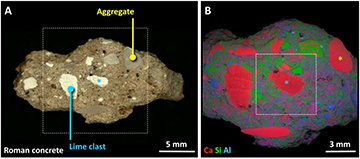
Under closer examination, these ancient samples also contain small, distinctive, millimeter-scale bright white mineral features, which have been long recognized as a ubiquitous component of Roman concretes. These white chunks, often referred to as “lime clasts,” originate from lime, another key component of the ancient concrete mix.
Upon further characterization of these lime clasts, using high-resolution multiscale imaging and chemical mapping techniques pioneered in Professor Admir Masic’s research lab at MIT, the researchers gained new insights into the potential functionality of these lime clasts.
Studying samples of this ancient concrete, he and his team determined that the white inclusions were made out of various forms of calcium carbonate. And spectroscopic examination provided clues that these had been formed at extreme temperatures, as would be expected from the exothermic reaction produced by using quicklime instead of, or in addition to, the slaked lime in the mixture. Hot mixing, the team has now concluded, was actually the key to the super-durable nature.
During the hot mixing process, the lime clasts develop a characteristically brittle nanoparticulate architecture, creating an easily fractured and reactive calcium source, which, as the team proposed, could provide a critical self-healing functionality. As soon as tiny cracks start to form within the concrete, they can preferentially travel through the high-surface-area lime clasts. This material can then react with water, creating a calcium-saturated solution, which can recrystallize as calcium carbonate and quickly fill the crack, or react with pozzolanic materials to further strengthen the composite material. These reactions take place spontaneously and therefore automatically heal the cracks before they spread. Previous support for this hypothesis was found through the examination of other Roman concrete samples that exhibited calcite-filled cracks.
To prove that this was indeed the mechanism responsible for the durability of the Roman concrete, the team produced samples of hot-mixed concrete that incorporated both ancient and modern formulations, deliberately cracked them, and then ran water through the cracks. Sure enough: Within two weeks the cracks had completely healed and the water could no longer flow. An identical chunk of concrete made without quicklime never healed, and the water just kept flowing through the sample. As a result of these successful tests, the team is working to commercialize this modified cement material.
Through the extended functional lifespan and the development of lighter-weight concrete forms, Masic hopes that these efforts could help reduce the environmental impact of cement production, which currently accounts for about 8% of global greenhouse gas emissions. Along with other new formulations, such as concrete that can actually absorb carbon dioxide from the air, another current research focus of the Masic lab, these improvements could help to reduce concrete’s global impact.
Image – Compositional and morphological characterization of ancient and modern lime clasts. (a) Optical micrographs showing the conspicuous bright white color of the lime clasts, which can easily be identified from large-area elemental mapping via SEM-EDS (b). Courtesy of Science Advances (2023). DOI: 10.1126/sciadv.add1602.
************
For more information:
Surprising speed-dependent friction with graphene
The speed at which an atomic force microscope moves across the surface of certain materials is influenced by the frictional properties of the substrate. One such example is graphene, which consists of a single layer of carbon atoms in a honeycomb arrangement. It is being examined with a view to potential use as a lubricating layer. Applications where a reduction of friction is desired include hard disks or moving components for satellites or space telescopes.
Previous studies have shown that a graphene ribbon can be moved across a gold surface with almost no friction. But if graphene is applied to a platinum surface, it has a significant impact on the measurable friction forces. Now, physicists from the University of Basel and Tel Aviv University have reported in the journal Nano Letters (“Velocity Dependence of Moiré Friction”) that, in this instance, the friction depends on the speed at which the tip of an atomic force microscope (AFM) is moved across the surface.
This finding is surprising because friction does not depend on speed according to Coulomb’s law, which applies in the macro world.
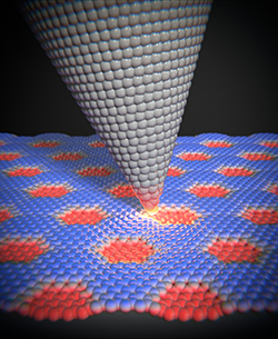
In conjunction with the platinum substrate, graphene no longer forms only the hexagonal honeycomb pattern of carbon atoms and instead forms superstructures known as Moiré superlattices. The surface is then no longer completely flat and exhibits a certain degree of roughness.
“If we move the AFM tip across this slightly corrugated surface at low speed, we measure a weak and almost constant frictional force,” explains Professor Ernst Meyer from the Swiss Nanoscience Institute and the Department of Physics at Basel University. “Above a certain threshold, however, the friction then increases with the speed of the AFM tip,” adds first author Dr. Yiming Song. “The larger the Moiré superstructure, the lower the threshold at which the friction becomes speed-dependent.”
The researchers found that there is greater resistance at the ridges of the Moiré superstructures during the movement of the tip. These ridges undergo elastic deformation due to the pushing tip before relaxing again when the pressure is sufficiently high. This effect results in greater frictional forces that increase with the speed of the tip. Simulations and an analytical model confirm the experimental findings obtained by this international team of researchers.
Image – The friction between the tip of an atomic force microscope and the Moiré superstructures depends on the speed at which the tip is moved across the surface. Courtesy of University of Basel.
************
For more information:
Milestone for light-driven electronics: excitons generated in a topological insulator for the first time
An international team of scientists collaborating within the Würzburg-Dresden Cluster of Excellence ct.qmat, Germany, has achieved a breakthrough in quantum research – the first detection of excitons (electrically neutral quasiparticles) in a topological insulator. This discovery paves the way for a new generation of light-driven computer chips and quantum technologies. It was enabled thanks to smart material design in Würzburg, the birthplace of topological insulators. The findings have been published in the journal Nature Communications.
In their search for novel materials for future quantum technologies, scientists from the Cluster of Excellence ct.qmat – Complexity and Topology in Quantum Matter – at the two universities in Würzburg and Dresden are concentrating on topological insulators, which enable the lossless conduction of electrical current and robust information storage. The first experimental realization of this materials class took place in Würzburg in 2007, prompting a worldwide research boom in solid-state physics that continues to this day.
Previous concepts for using topological insulators are based on the application of electrical voltages in order to control currents – an approach adopted from conventional computer chips. However, if the exotic material properties are based on electrically neutral particles (which are neither positively nor negatively charged), an electric voltage no longer works. Such quantum phenomena therefore require other tools if they are to be generated at all – for example, light.
An international research team headed by Professor Ralph Claessen, quantum physicist from Würzburg and co-spokesperson of ct.qmat, has now made a crucial discovery. “For the first time, we’ve been able to generate and experimentally detect quasiparticles known as excitons in a topological insulator. We’ve thus created a new toolkit for solid-state physics that can be used to control electrons optically.” As Claessen emphasizes, “This principle could become the basis for a new type of electronic components.”
Excitons are electronic quasiparticles. Although they seem to behave like independent particles, they actually represent an excited electronic state that can only be generated in certain types of quantum matter. “We created excitons by applying a short light pulse to a thin film consisting of just one single layer of atoms,” explains Claessen. What’s unusual about this, he says, is that the excitons were activated in a topological insulator – something that wasn’t possible before. “This has opened up a completely new line of research for topological insulators,” adds Claessen.
The right starting material is crucial – in this case bismuthene. “It’s the heavy sibling of the miracle material graphene,” says Claessen, who first tailored the topological insulator in the lab five years ago. “We’re the global leaders in this field,” he adds. “Due to our sophisticated materials design, the atoms of the single layer of bismuthene are arranged in a honeycomb pattern, just like graphene. The difference is that bismuthene’s heavy atoms make it a topological insulator, meaning it can conduct electricity along the edge without loss – even at room temperature. This can’t be done by graphene.”
For about ten years, excitons have been investigated in other two-dimensional semiconductors and regarded as information carriers for light-driven components. “For the first time, we’ve managed to optically excite excitons in a topological insulator. The interaction between light and excitons means we can expect new phenomena in such materials. This principle could be used, for example, to generate qubits,” says Claessen.
Qubits are computing units for quantum chips. They’re far superior to traditional bits and allow to solve tasks within minutes for which conventional supercomputers would literally take years.i Using light instead of electrical voltage enables quantum chips with much faster processing speeds. The latest findings therefore pave the way for future quantum technologies and a new generation of light-driven devices in microelectronics.
Image – Three excitons (pairs consisting of an electron and an electron hole) on the topological insulator bismuthene. Due to the honeycomb atomic structure, electrons can only flow along the edges. This topological effect allows current to flow without resistance. Researchers from ct.qmat have managed to generate excitons in a topological insulator for the very first time, paving the way for novel light-driven components – and possibly even the realization of qubits. Courtesy of Jörg Bandmann/ct.qmat.
For more information:
Würzburg-Dresden Cluster of Excellence ct.qmat
Imec enables tight standard cell boundary scaling using a two-level semi-damascene integration scheme
Imec, Belgium, a world-leading research and innovation hub in nanoelectronics and digital technologies, presents a semi-damascene integration approach for implementing the vertical-horizontal-vertical (VHV) scaling booster – intended to enable 4-track (4T) standard cells. The semi-damascene process enables cell boundary scaling down to 8nm tip-to-tip (T2T) in the middle-of-line (MOL) layers, providing self-aligned edges.
This provides a booster that designers can use for packing standard cells tighter, representing a 21 percent area gain over 5T designs. The novel routing scheme, along with the semi-damascene integration approach, will be critical to gradually push the logic scaling roadmap well into the Å era.
For a long time, the MOL, which provides the connection between the front-end-of-line (FEOL) and back-end-of-line (BEOL), has been organized as a single-layer contact. But currently, it is expanding into several layers, including, for example, the Mint and Vint layers. These MOL layers carry the electrical signals from the transistor’s source, drain, and gate to the local interconnects and vice versa.
Imec recently introduced a novel standard cell routing architecture called VHV, which involves the introduction of an extra MOL layer (M0B) as a scaling booster to enable 4T standard cell designs. With this booster, the first three routing layers in the standard cell follow a VHV routing style instead of the traditional HVH routing style in 5T standard cells. However, the novel two-level MOL VHV scaling booster is challenging from a process integration point of view, mainly arising from the tight boundary between neighboring 4T standard cells. The cell boundary requires a tight T2T between adjacent MOL M0B lines and two vias (VintB) facing each other with well-defined via edges – all at a minimum distance of one critical dimension (CD) of the top Mint layer. This means that the T2T and VintB via distance will need to be gradually reduced from ~24nm to ~8nm for upcoming technology nodes. This can no longer be achieved using a direct lithographic print but requires a self-aligned patterning strategy instead.
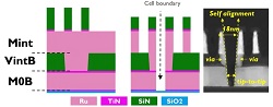
Researchers defined the tight boundary between adjacent standard cells using a two-level semi-damascene approach involving a direct metal etch. Zsolt Tőkei, program director of nano-interconnects and fellow at imec said, “Roughly speaking, we start from conventionally defined continuous lines and wider vias and, once two metal layers are finished, we split them into two, using the top 16-18nm pitch Mint layer as a hard mask for the final patterning step. This results in 3 edges (of Mint, VintB, and M0B) that are simultaneously self-aligned. With our Ru-based two-level test vehicle, we obtained an average via CD of 10.5nm and M0B T2T as tight as 8.9nm – a key achievement.” Imec researchers complemented structural validation with an initial electrical characterization of line resistance and isolation properties.
“The VHV routing scheme is a critical scaling booster to enable cell boundaries at the A10, A7, A5, A3 technology nodes,” adds Tőkei. “It also applies to future device architectures such as nanosheet, forksheet, and CFET. By extending semi-damascene from the BEOL towards the MOL, we have now also found a way to integrate this promising booster. More detailed investigations will, however, be needed, and for that purpose, imec is taping out a new dedicated mask.”
Image – (Left/middle) Schematic representation of the semi-damascene process flow used to test the key features of VHV. (Right) TEM image of the test vehicle after the final Ru etch: T2T M0B and VintB via are self-aligned to the 18mn pitch Mint layer.
For more information:
Imec
Blocking radio waves and electromagnetic interference with the flip of a switch
Researchers in Drexel University’s College of Engineering have developed a thin film device fabricated by spray coating that can block electromagnetic radiation with the flip of a switch. The breakthrough, enabled by versatile two-dimensional materials called MXenes, could adjust the performance of electronic devices, strengthen wireless connections, and secure mobile communications against intrusion.
The team previously demonstrated that two-dimensional layered MXene materials – discovered just over a decade ago – when combined with an electrolyte solution, can be turned into a potent active shield against electromagnetic waves. This latest MXene discovery, reported in Nature Nanotechnology, shows how this shielding can be tuned when a small voltage – less than that produced by an alkaline battery – is applied.
MXene is a unique material in that it is highly conductive making it perfectly suited for reflecting microwave radiation that could cause static, feedback, or diminish the performance of communications devices. But its internal chemical structure can also be temporarily altered to allow these electromagnetic waves to pass through.
This means that a thin coating on a device or electrical components prevents them from both emitting electromagnetic waves, as well as being penetrated by those emitted by other electronics. Eliminating the possibility of interference from both internal and external sources can ensure the performance of the device, but some waves must be allowed to exit and enter when it is being used for communication.
The key to eliciting bidirectional tunability of MXene’s shielding property is using the flow and expulsion of ions to alternately expand and compress the space between material’s layers, like an accordion, as well as to change the surface chemistry of MXenes.
With a small voltage applied to the film, ions enter – or intercalate – between the MXene layers altering the charge of their surface and inducing electrostatic attraction, which serves to change the layer spacing, the conductivity and shielding efficiency of the material. When the ions are deintercalated as the current is switched off, the MXene layers return to their original state.
The team tested 10 different MXene-electrolyte combinations, applying each via paint sprayer in a layer about 30 to 100 times thinner than a human hair. The materials consistently demonstrated the dynamic tunability of shielding efficiency in blocking microwave radiation, which is impossible for traditional metals like copper and steel. And the device sustained the performance through more than 500 charge-discharge cycles.
These results indicate that the MXene films can convert from electromagnetic interference shielding to quasi-electromagnetic wave transmission by electrochemical oxidation of MXenes. The MXene film can potentially serve as a dynamic EMI shielding switch.
For security applications, the team suggests that the MXene shielding could hide devices from detection by radar or other tracing systems. The team also tested the potential of a one-way shielding switch. This would allow a device to remain undetectable and protected from unauthorized access until it is deployed for use.
The next step for the team is to explore additional MXene-electrolyte combinations and mechanisms to fine-tune the shielding to achieve a stronger modulation of electromagnetic wave transmission and dynamic adjustment to block radiation at a variety of bandwidths.
For more information:
Drexel University


Synopsys, Inc., Mountain View, Calif., reaches scale for AI-driven chip designs as major semiconductor customers register the first 100 commercial tape-outs with the company’s award-winning Synopsys DSO.ai autonomous design system. Recent customers, including STMicroelectronics and SK hynix, have all seen significant uplifts in productivity and PPA, and are now charting a new design course using reinforcement learning-enabled design tools on cloud and on-premise.
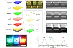
MIT engineers, Boston, Mass., have developed a new way to make sharper, defect-free displays, stacking the diodes to create vertical, multicolored pixels. Each stacked pixel can generate the full commercial range of colors and measures about 4 microns wide. The microscopic pixels, or micro-LEDs, can be packed to a density of 5,000 pixels per inch.
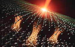
Researchers at the Department of Energy’s Lawrence Berkeley National Laboratory (Berkeley Lab), Berkeley, Calif., discover that electrons play a surprising role in heat transfer between layers of semiconductors, with implications for next-generation electronic devices.